- 您現在的位置:買賣IC網 > PDF目錄371046 > MC68B912B32FU8 (MOTOROLA INC) 16-Bit Microcontroller PDF資料下載
參數資料
| 型號: | MC68B912B32FU8 |
| 廠商: | MOTOROLA INC |
| 元件分類: | 微控制器/微處理器 |
| 英文描述: | 16-Bit Microcontroller |
| 中文描述: | 16-BIT, FLASH, 8 MHz, MICROCONTROLLER, PQFP80 |
| 封裝: | QFP-80 |
| 文件頁數: | 34/128頁 |
| 文件大小: | 748K |
| 代理商: | MC68B912B32FU8 |
第1頁第2頁第3頁第4頁第5頁第6頁第7頁第8頁第9頁第10頁第11頁第12頁第13頁第14頁第15頁第16頁第17頁第18頁第19頁第20頁第21頁第22頁第23頁第24頁第25頁第26頁第27頁第28頁第29頁第30頁第31頁第32頁第33頁當前第34頁第35頁第36頁第37頁第38頁第39頁第40頁第41頁第42頁第43頁第44頁第45頁第46頁第47頁第48頁第49頁第50頁第51頁第52頁第53頁第54頁第55頁第56頁第57頁第58頁第59頁第60頁第61頁第62頁第63頁第64頁第65頁第66頁第67頁第68頁第69頁第70頁第71頁第72頁第73頁第74頁第75頁第76頁第77頁第78頁第79頁第80頁第81頁第82頁第83頁第84頁第85頁第86頁第87頁第88頁第89頁第90頁第91頁第92頁第93頁第94頁第95頁第96頁第97頁第98頁第99頁第100頁第101頁第102頁第103頁第104頁第105頁第106頁第107頁第108頁第109頁第110頁第111頁第112頁第113頁第114頁第115頁第116頁第117頁第118頁第119頁第120頁第121頁第122頁第123頁第124頁第125頁第126頁第127頁第128頁
MOTOROLA
34
MC68HC912B32
MC68HC912B32TS/D
This register is associated with external bus control signals and interrupt inputs including data bus en-
able (DBE), mode select (MODB/IPIPE1, MODA/IPIPE0), E clock, data size (LSTRB/TAGLO), read/
write (R/W), IRQ, and XIRQ. When the associated pin is not used for one of these specific functions,
the pin can be used as general-purpose I/O. The port E assignment register (PEAR) selects the function
of each pin. DDRE determines the primary direction of each port E pin when configured to be general-
purpose I/O.
Some of these pins have software selectable pull-ups (DBE, LSTRB, R/W, and XIRQ). A single control
bit enables the pull-ups for all these pins which are configured as inputs. IRQ always has a pull-up.
This register is not in the map in peripheral mode or expanded modes when the EME bit is set.
Read and write anytime.
This register determines the primary direction for each port E pin configured as general-purpose I/O.
0 = Associated pin is a high-impedance input
1 = Associated pin is an output
PE[1:0] are associated with XIRQ and IRQ and cannot be configured as outputs. These pins can be
read regardless of whether the alternate interrupt functions are enabled.
This register is not in the map in peripheral mode and expanded modes while the EME control bit is set.
Read and write anytime.
The PEAR register is used to choose between the general-purpose I/O functions and the alternate bus
control functions of port E. When an alternate control function is selected, the associated DDRE bits are
overridden.
The reset condition of this register depends on the mode of operation because bus-control signals are
needed immediately after reset in some modes.
In normal single-chip mode, no external bus control signals are needed so all of port E is configured for
general-purpose I/O.
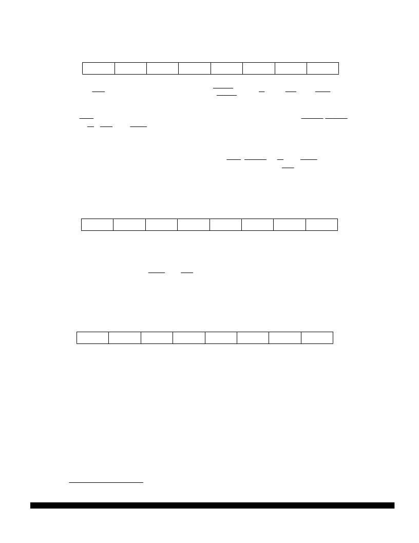
PORTE —
Port E Register
$0008
Bit 7
6
5
4
3
2
1
Bit 0
Single Chip
PE7
PE6
PE5
PE4
PE3
PE2
PE1
PE0
RESET:
–
–
–
–
–
–
–
–
Alt. Pin
Function
DBE
MODB or
IPIPE1
MODA or
IPIPE0
ECLK
LSTRB or
TAGLO
R/W
IRQ
XIRQ
DDRE —
Port E Data Direction Register
$0009
Bit 7
6
5
4
3
2
1
Bit 0
DDE7
DDE6
DDE5
DDE4
DDE3
DDE2
0
0
RESET:
0
0
0
0
0
0
–
–
PEAR —
Port E Assignment Register
$000A
Bit 7
6
5
4
3
2
1
Bit 0
NDBE
0
PIPOE
NECLK
LSTRE
RDWE
0
0
RESET:
0
–
0
0
0
0
–
–
Normal
Expanded
RESET:
0
–
1
0
1
1
–
–
Special
Expanded
RESET:
1
–
0
1
0
0
–
–
Peripheral
RESET:
1
–
0
1
0
0
–
–
Normal
Single Chip
RESET:
0
–
1
0
1
1
–
–
Special
Single Chip
相關PDF資料 |
PDF描述 |
|---|---|
| MC68C912B32CFU8 | 16-Bit Microcontroller |
| MC68CK338 | Highly Integrated, Low-Power, 32-Bit Microcontroller |
| MC68EC060 | 32-Bit Microprocessors.(32位微處理器) |
| MC68EN360RC25V | QUad Integrated Communications Controller Users Manual |
| MC68EN360CFE25 | QUad Integrated Communications Controller Users Manual |
相關代理商/技術參數 |
參數描述 |
|---|---|
| MC68BOOL | 制造商:MOTOROLA 制造商全稱:Motorola, Inc 功能描述:8-BIT MICROPROCESSING UNIT (MPU) |
| MC68BOOP | 制造商:MOTOROLA 制造商全稱:Motorola, Inc 功能描述:8-BIT MICROPROCESSING UNIT (MPU) |
| MC68BOOS | 制造商:MOTOROLA 制造商全稱:Motorola, Inc 功能描述:8-BIT MICROPROCESSING UNIT (MPU) |
| MC68C812A4 | 制造商:FREESCALE 制造商全稱:Freescale Semiconductor, Inc 功能描述:Technical Supplement MC68C812A4 3.3V Electrical Characteristics |
| MC68C912B32CFU8 | 制造商:MOTOROLA 制造商全稱:Motorola, Inc 功能描述:16-Bit Microcontroller |
發布緊急采購,3分鐘左右您將得到回復。