- 您現在的位置:買賣IC網 > PDF目錄382382 > PCF5083 (NXP Semiconductors N.V.) STEEL COVER PDF資料下載
參數資料
| 型號: | PCF5083 |
| 廠商: | NXP Semiconductors N.V. |
| 英文描述: | STEEL COVER |
| 中文描述: | GSM信號處理IC |
| 文件頁數: | 60/136頁 |
| 文件大小: | 602K |
| 代理商: | PCF5083 |
第1頁第2頁第3頁第4頁第5頁第6頁第7頁第8頁第9頁第10頁第11頁第12頁第13頁第14頁第15頁第16頁第17頁第18頁第19頁第20頁第21頁第22頁第23頁第24頁第25頁第26頁第27頁第28頁第29頁第30頁第31頁第32頁第33頁第34頁第35頁第36頁第37頁第38頁第39頁第40頁第41頁第42頁第43頁第44頁第45頁第46頁第47頁第48頁第49頁第50頁第51頁第52頁第53頁第54頁第55頁第56頁第57頁第58頁第59頁當前第60頁第61頁第62頁第63頁第64頁第65頁第66頁第67頁第68頁第69頁第70頁第71頁第72頁第73頁第74頁第75頁第76頁第77頁第78頁第79頁第80頁第81頁第82頁第83頁第84頁第85頁第86頁第87頁第88頁第89頁第90頁第91頁第92頁第93頁第94頁第95頁第96頁第97頁第98頁第99頁第100頁第101頁第102頁第103頁第104頁第105頁第106頁第107頁第108頁第109頁第110頁第111頁第112頁第113頁第114頁第115頁第116頁第117頁第118頁第119頁第120頁第121頁第122頁第123頁第124頁第125頁第126頁第127頁第128頁第129頁第130頁第131頁第132頁第133頁第134頁第135頁第136頁
1996 Oct 29
60
Philips Semiconductors
Objective specification
GSM signal processing IC
PCF5083
9.1.9
P
OWER SAVING MODES
9.1.9.1
Idle mode
When operating in Idle mode the DSP enters a dormant
state and requires only a fraction of the power normally
needed to supply the device in the full operating mode.
The processor core is switched off whereas the I/O section
of the processor is fully functional. The Idle mode is
invoked by the on-chip firmware whenever the DSP is
waiting for an I/O event. The DSP automatically leaves the
Idle mode as soon as the input or output operation has
been completed.
9.1.9.2
Power-down mode
The Power-down mode is initiated when the signal
DSPON is deactivated during Sleep mode (see
Section 8.3.3). The DSP will stop operation synchronously
after a maximum of 3 CLKI cycles delay. All parts of the
DSP which operate with the main processor clock are in
static state. Only the blocks running with the serial
interface clocks are not affected by the Power-down mode.
For minimum power consumption the external serial shift
clocks should therefore be switched off. The DSP remains
in the power-down state as long as the signal DSPON is
held inactive. The processor continues its operation for a
maximum of 3 clock cycles after the signal DSPON is set
active again.
9.2
Message Interface to the System Controller
The DSP can be controlled with commands and joining
16-bits parameters from the System Controller via the host
port register PI. The first word always contains the
command OPCODE and length. The second word is an
arbitrary ID code which is useful for debugging purposes.
The following words are command parameters. The DSP
can also generate indications giving status information or
requested data. These indication messages can be read
(R) via host port register PO.
The DMA message is used to download data into the
program/data RAM. Download is always done into the
data address space. The parameters mc_before and
mc_after indicate the value of the Memory Configuration
Register before and after download. Thus, it is possible to
switch a RAM bank into the data address space, download
a program and switch it back afterwards. For more
information about the MC Register and the PCF5083
memory mapping please refer to “Information Manual
Digital Signal Processors PCF508x, Philips
Semiconductors, 1995”
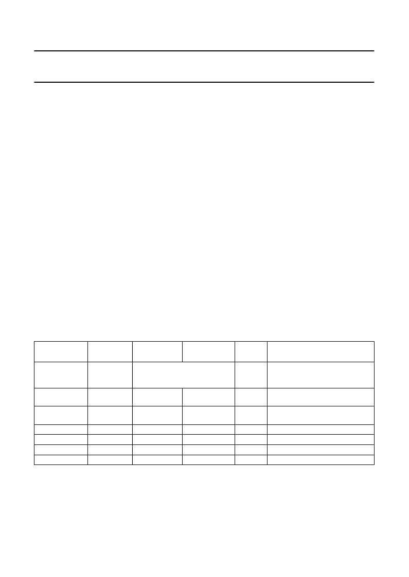
Table 52
Commands/indications to/from the PCF5083
Note
1.
X = don’t care.
MNEMONIC
DIRECTION
OPCODE
(1)
bit 15 to bit 8
LENGTH
bit 7 to bit 0
ID
DATA
DMA
write
0X0000
msg_id
mc_before n_words;
address data [1] to data [n words];
mc_after
proc_id;
parameter_1 to parameter_N
proc_id;
return_value 1 to return value_N
cmd_1 to cmd_N
reset_parm
data_1 to data_N
error_code
EXEC_PROC
write
0X01
3 + npar
msg_id
PROC_RETUR
N
PACKET
RESET
NOP
ERROR
read
0X11
3 + n_retvals
msg_id
write
write
write
read
0X02
0X03
0X05
0X12
2 + N (cmd_len)
3
2 + N
3
msg_id
msg_id
msg_id
msg_id
相關PDF資料 |
PDF描述 |
|---|---|
| PCF84C12A | 8-BIT MICROCONTROLLER |
| PCF84C12AP | 8-BIT MICROCONTROLLER |
| PCF84C12AT | 8-BIT MICROCONTROLLER |
| PCF84C21A | Telecom microcontrollers |
| PCF84C41A | Telecom microcontrollers |
相關代理商/技術參數 |
參數描述 |
|---|---|
| PCF5083H/001/F2 | 制造商:PHILIPS 制造商全稱:NXP Semiconductors 功能描述:GSM signal processing IC |
| PCF5083H/5V2/F3 | 制造商:PHILIPS 制造商全稱:NXP Semiconductors 功能描述:GSM signal processing IC |
| PCF5083H/F2 | 制造商:PHILIPS 制造商全稱:NXP Semiconductors 功能描述:GSM signal processing IC |
| PCF51AC128ACFUE | 功能描述:32位微控制器 - MCU 32 Bit 128K FLASH 32K RAM CAN EN RoHS:否 制造商:Texas Instruments 核心:C28x 處理器系列:TMS320F28x 數據總線寬度:32 bit 最大時鐘頻率:90 MHz 程序存儲器大小:64 KB 數據 RAM 大小:26 KB 片上 ADC:Yes 工作電源電壓:2.97 V to 3.63 V 工作溫度范圍:- 40 C to + 105 C 封裝 / 箱體:LQFP-80 安裝風格:SMD/SMT |
| PCF51AC128ACLKE | 功能描述:32位微控制器 - MCU 32 Bit 128K FLASH 32K RAM CAN EN RoHS:否 制造商:Texas Instruments 核心:C28x 處理器系列:TMS320F28x 數據總線寬度:32 bit 最大時鐘頻率:90 MHz 程序存儲器大小:64 KB 數據 RAM 大小:26 KB 片上 ADC:Yes 工作電源電壓:2.97 V to 3.63 V 工作溫度范圍:- 40 C to + 105 C 封裝 / 箱體:LQFP-80 安裝風格:SMD/SMT |
發布緊急采購,3分鐘左右您將得到回復。