- 您現在的位置:買賣IC網 > PDF目錄373969 > AD9854 (Analog Devices, Inc.) CMOS 300MHz Quadrature Complete-DDS PDF資料下載
參數資料
| 型號: | AD9854 |
| 廠商: | Analog Devices, Inc. |
| 元件分類: | XO, clock |
| 英文描述: | CMOS 300MHz Quadrature Complete-DDS |
| 中文描述: | 300MHz CMOS正交DDS數字合成器 |
| 文件頁數: | 11/28頁 |
| 文件大小: | 589K |
| 代理商: | AD9854 |
第1頁第2頁第3頁第4頁第5頁第6頁第7頁第8頁第9頁第10頁當前第11頁第12頁第13頁第14頁第15頁第16頁第17頁第18頁第19頁第20頁第21頁第22頁第23頁第24頁第25頁第26頁第27頁第28頁

AD9854 PRELIMINARY TECHNICAL DATA
_____________________________________________________________________________________________________
The PLL function can be bypassed to allow direct
clocking of the AD9854 from an external clock source.
The
system clock
for the AD9854 is either the output
of the REFCLK Multiplier (if it is engaged) or the
REFCLK inputs. REFCLK may be either a single-
ended or differential input by setting pin 64,
Diff Clk
Enable,
low or high respectively.
7/16/99 REV.PRA
11
A “
PLL Range
” bit in the control register (address 1E
hex) allows the VCO “gain” to be increased (logic
high) or decreased (logic low). Decreased gain means
that the VCO becomes less responsive to changes in
control voltage. Increased gain makes the VCO more
responsive to changes in control voltage and will
increase the VCO frequency range. Any noise on the
VCO control voltage line will cause an increase in
phase noise of the oscillator. If the VCO gain is
increased, then phase noise will increase as well. The
default value of this bit is logic high – highest gain – to
accommodate a maximum clock speed of 300 MHz. If
the system clock is to be less than 200 MHz, it is best
to set this bit low for best phase noise performance.
Pin 61.
PLL Filter
, is the connection for an external
RC loop filter consisting of a 1.3k resistor in series
with a .01
μ
F capacitor tied to 3.3 volts. The filter is
user supplied and must be present for proper REFCLK
Multiplier functioning. The filter is connected directly
to the PLL phase detector charge pump output stage.
Users should exercise care to avoid injecting noise onto
this line that controls the VCO output frequency.
When REFCLK multiplier is not needed it can be
powered-down by setting the
PLL POWER-DOWN
bit high or by-passed by setting the “
Bypass PLL
” bit
high in control register address 1D and 1E (hex)
respectively.
Differential REFCLK Enable:
Bringing pin 64 high
enables the differential clock mode. In this mode,
REFCLK and REFCLKB (pins 69 and 68) are
assumed to carry clock signals (3.3V CMOS logic
levels or 1V p-p dc offset (to Vdd) sine waves)
whose phases differ by 180 degrees. Differential clock
signals are preferred over single-ended clocking of the
AD9854/52.
When pin 64 (Diff Clk Enable) is tied low, REFCLK
(pin 69) is the only active clock input. This is referred
to as the
single-ended
mode. In this mode, pin 68
(REFCLKB) should be tied low or high but not left
floating.
Parallel/Serial programming mode -
setting pin 70
high invokes parallel mode, whereas setting pin 70 low
will invoke the serial programming mode. Refer to the
extensive description of the serial and parallel
programming protocol elsewhere in this data sheet.
Two control bits located at address 20 hex in the
Register Layout table apply only to the serial
programming mode.
LSB First
when high dictates that serial data will be
loaded starting with the LSB of the word. When low
(the default value) serial data is loaded starting with
the MSB of the word.
SDO Active
when high
indicates that the SDO pin, Pin 18, is dedicated to
reading back data from the AD9854 registers. When
SDO Active is low (default value), this indicates that
the SDIO pin, Pin 19 acts as a bi-directional serial data
input and output pin and Pin 18 has no function in the
serial mode.
Modes of Operation –
single-tone, FSK, ramped
FSK, CHIRP and PSK modes are selected according to
three MODE bits in control register 1F (hex) in the
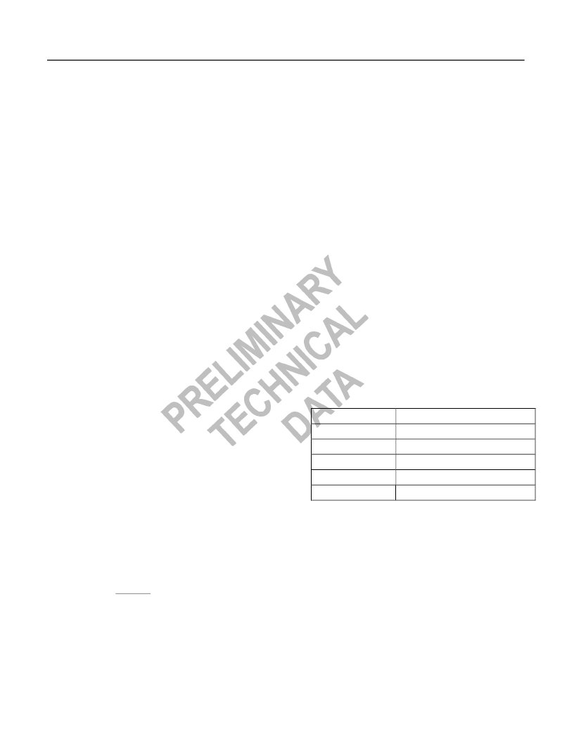
Register Layout Table. The following table applies:
M[2] M[1] M[0]
0 0 0
0 0 1
0 1 0
0 1 1
1 0 0
FUNCTION INVOKED
Single-tone
Frequency-shift keying (FSK)
Ramped FSK
CHIRP
Phase-shift keying (BPSK)
Each mode will initially use the default conditions that
are invoked upon power-up and Master Reset. The
default conditions setup a “do-nothing” state at the
DAC outputs (0 Hz, 0 degrees phase, minimum
amplitude. A brief discussion of each mode, associated
programming registers and control bits follows:
Single-Tone Mode:
This is the default mode
after a master reset. The frequency is
determined by the 48-bit Frequency Tuning
Word 1 register at address 4 – 9 hex, and the
phase is set in 14-bit Phase Adjust Register 1
at address 0-1 hex. I & Q output amplitude
can be adjusted in 12-bit registers located at
相關PDF資料 |
PDF描述 |
|---|---|
| AD9858TLPCB | 1 GSPS Direct Digital Synthesizer |
| AD9858BSV | 1 GSPS Direct Digital Synthesizer |
| AD9858PCB | 1 GSPS Direct Digital Synthesizer |
| AD9858 | 1 GSPS Direct Digital Synthesizer |
| AD9858FDPCB | 1 GSPS Direct Digital Synthesizer |
相關代理商/技術參數 |
參數描述 |
|---|---|
| AD9854/PCB | 制造商:Analog Devices 功能描述:Evaluation Board For IC Digital Synthesizer Single 制造商:Analog Devices 功能描述:Direct Digital Synthesizer IC (DDS) |
| AD9854/PCBZ | 功能描述:BOARD EVAL FOR AD9854 RoHS:是 類別:編程器,開發系統 >> 評估演示板和套件 系列:AgileRF™ 標準包裝:1 系列:PCI Express® (PCIe) 主要目的:接口,收發器,PCI Express 嵌入式:- 已用 IC / 零件:DS80PCI800 主要屬性:- 次要屬性:- 已供物品:板 |
| AD9854ASQ | 制造商:Analog Devices 功能描述:IC DDS SYNTHESIZER |
| AD9854ASQZ | 制造商:Analog Devices 功能描述:Direct Digital Synthesizer 300MHz 2-DAC 12-Bit Parallel/Serial 80-Pin LQFP 制造商:Analog Devices 功能描述:Communication IC |
| AD9854AST | 制造商:Analog Devices 功能描述:Direct Digital Synthesizer 300MHz 2-DAC 12-Bit Parallel/Serial 80-Pin LQFP Tray 制造商:Rochester Electronics LLC 功能描述:200 MHZ QUADRATURE DDS SYNTHESIZER - Tape and Reel 制造商:Analog Devices 功能描述:IC SEMICONDUCTOR ((NS)) |
發布緊急采購,3分鐘左右您將得到回復。