- 您現(xiàn)在的位置:買賣IC網(wǎng) > PDF目錄373969 > AD9854 (Analog Devices, Inc.) CMOS 300MHz Quadrature Complete-DDS PDF資料下載
參數(shù)資料
| 型號: | AD9854 |
| 廠商: | Analog Devices, Inc. |
| 元件分類: | XO, clock |
| 英文描述: | CMOS 300MHz Quadrature Complete-DDS |
| 中文描述: | 300MHz CMOS正交DDS數(shù)字合成器 |
| 文件頁數(shù): | 6/28頁 |
| 文件大小: | 589K |
| 代理商: | AD9854 |
第1頁第2頁第3頁第4頁第5頁當(dāng)前第6頁第7頁第8頁第9頁第10頁第11頁第12頁第13頁第14頁第15頁第16頁第17頁第18頁第19頁第20頁第21頁第22頁第23頁第24頁第25頁第26頁第27頁第28頁
AD9854 PRELIMINARY TECHNICAL DATA
_____________________________________________________________________________________________________
7/16/99 REV.PRA
6
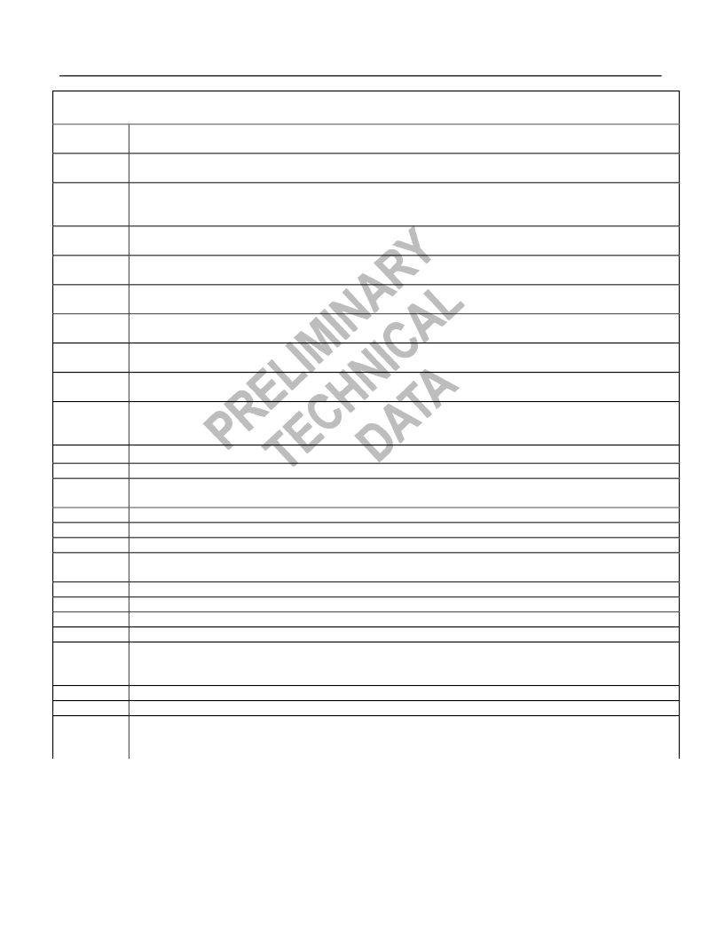
Table I. AD9854 PIN FUNCTION DESCRIPTIONS
REFCLK
Pin 69. Single-ended reference clock input or one of two differential clock signals. Normal 3.3V CMOS logic
levels or 1V p-p sine wave centered about +1.6V.
Pin 68. The complementary (180 degrees out of phase) differential clock signal. User should tie this pin high
or low when single-ended clock mode is selected. Same signal levels as REFCLK above.
Pin 64. Digital input to select either differential (logic high) or single-ended (logic low) reference clock mode.
In the single-ended mode, pin 68 above is switched out of the clock path, and pin 69 assumes total control of
the REFCLK function. In differential mode, both pins 68 and 69 work together to provide REFCLK function.
Pin 56. Common connection for both I and Q DAC’s to set the full-scale output current. R
SET
= 39.9/Iout.
Normal R
SET
range
is from 8k (5 mA) to 2k (20 mA).
Pin 55. Common by-pass capacitor connection for both I and Q DAC’s. A .01
μ
F chip cap from this pin to
AVDD improves harmonic distortion and SFDR slightly. No connect is permissible (slight SFDR degradation).
Pins 33, 34, 39, 40, 41, 45, 46, 47, 53, 59, 62, 66, 67. Connections for analog circuitry ground return. Same
potential as D
GND
Pins 11, 12, 26, 27, 28, 72, 75, 76, 77, 78 . Connections for digital circuitry ground return. Same potential as
A
GND
Pins 31, 32, 37, 38, 44, 50, 54, 60, 65. Connections for the analog circuitry supply voltage. Nominally 3.3
volts more positive than A
GND
and D
GND
.
Pins 9, 10, 23, 24, 25, 73, 74, 79, 80. Connections for the digital circuitry supply voltage. Nominally 3.3 volts
more positive than A
GND
and D
GND
.
Pin 71. Initializes the serial/parallel programming bus to prepare for user programming; sets programming
registers to a “do-nothing” state defined by the default values seen in the
Register Layout
table. Active on
logic high . Asserting MASTER RESET is essential for proper operation upon power-up.
Pin 48. Unipolar current output of the I or Sine DAC.
Pin 49. Complementary unipolar current output of the I or Sine DAC.
Pin 52. Unipolar current output of the Q or Cosine DAC. This DAC can be programmed to accept external 12-
bit data in lieu of internal Cosine data. This allows the AD9854 to emulate the AD9852 control DAC function.
Pin 51. Complementary unipolar current output of the Q or Cosine or “control” DAC.
Pin 42. Voltage input positive. The internal high-speed comparator’s non-inverting input.
Pin 43. Voltage input negative. The internal high-speed comparator’s inverting input.
Pin 36. Internal high-speed comparator’s non-inverted output pin. Designed to drive 10 dBm to 50-ohm load
as well as standard CMOS logic levels.
Pins 13, 35, 57, 58, 63. No internal connection.
Pins 1 – 8. 8-bit bi-directional parallel programming data inputs. Used only in Parallel Programming mode.
Pin 21. Write parallel data to programming registers. Shared function with SCLK below.
Pin 22. Read parallel data from programming registers. Shared function with CSB below.
Pins 14 – 19. 6-bit parallel address inputs for Program Registers. Used only in Parallel Programming mode.
A0, A1 and A2 have a second function when the Serial Programming mode is selected. See immediately
below.
Pin 19. Bi-directional serial data input/output for use in 2-wire serial communication mode.
Pin 18. Uni-directional serial data output for use in 3-wire serial communication mode.
Pin 17. Allows a RESET of the serial communications bus that is unresponsive due to improper programming
protocol. Resetting the serial bus in this manner does not affect previous programming nor does it invoke the
“default” programming values seen in the
Register Layout
table. Active HIGH.
REFCLKB
DIFF CLK
ENABLE
DAC R
SET
DACBP
A
GND
D
GND
A
VDD
D
VDD
MASTER
RESET
IOUT1
IOUT1B
IOUT2
IOUT2B
VINP
VINN
VOUT
nc
D7 – D0
WRB
RDB
A5 – A0
SDIO
SDO
I/O RESET
相關(guān)PDF資料 |
PDF描述 |
|---|---|
| AD9858TLPCB | 1 GSPS Direct Digital Synthesizer |
| AD9858BSV | 1 GSPS Direct Digital Synthesizer |
| AD9858PCB | 1 GSPS Direct Digital Synthesizer |
| AD9858 | 1 GSPS Direct Digital Synthesizer |
| AD9858FDPCB | 1 GSPS Direct Digital Synthesizer |
相關(guān)代理商/技術(shù)參數(shù) |
參數(shù)描述 |
|---|---|
| AD9854/PCB | 制造商:Analog Devices 功能描述:Evaluation Board For IC Digital Synthesizer Single 制造商:Analog Devices 功能描述:Direct Digital Synthesizer IC (DDS) |
| AD9854/PCBZ | 功能描述:BOARD EVAL FOR AD9854 RoHS:是 類別:編程器,開發(fā)系統(tǒng) >> 評估演示板和套件 系列:AgileRF™ 標(biāo)準(zhǔn)包裝:1 系列:PCI Express® (PCIe) 主要目的:接口,收發(fā)器,PCI Express 嵌入式:- 已用 IC / 零件:DS80PCI800 主要屬性:- 次要屬性:- 已供物品:板 |
| AD9854ASQ | 制造商:Analog Devices 功能描述:IC DDS SYNTHESIZER |
| AD9854ASQZ | 制造商:Analog Devices 功能描述:Direct Digital Synthesizer 300MHz 2-DAC 12-Bit Parallel/Serial 80-Pin LQFP 制造商:Analog Devices 功能描述:Communication IC |
| AD9854AST | 制造商:Analog Devices 功能描述:Direct Digital Synthesizer 300MHz 2-DAC 12-Bit Parallel/Serial 80-Pin LQFP Tray 制造商:Rochester Electronics LLC 功能描述:200 MHZ QUADRATURE DDS SYNTHESIZER - Tape and Reel 制造商:Analog Devices 功能描述:IC SEMICONDUCTOR ((NS)) |
發(fā)布緊急采購,3分鐘左右您將得到回復(fù)。