- 您現在的位置:買賣IC網 > PDF目錄373970 > AD9898KCPRL-20 (ANALOG DEVICES INC) TVPS00RF-21-41S W/ PC CON PDF資料下載
參數資料
| 型號: | AD9898KCPRL-20 |
| 廠商: | ANALOG DEVICES INC |
| 元件分類: | 消費家電 |
| 英文描述: | TVPS00RF-21-41S W/ PC CON |
| 中文描述: | SPECIALTY CONSUMER CIRCUIT, QCC48 |
| 封裝: | MO-220-VKKD-2, LFCSP-48 |
| 文件頁數: | 17/52頁 |
| 文件大小: | 557K |
| 代理商: | AD9898KCPRL-20 |
第1頁第2頁第3頁第4頁第5頁第6頁第7頁第8頁第9頁第10頁第11頁第12頁第13頁第14頁第15頁第16頁當前第17頁第18頁第19頁第20頁第21頁第22頁第23頁第24頁第25頁第26頁第27頁第28頁第29頁第30頁第31頁第32頁第33頁第34頁第35頁第36頁第37頁第38頁第39頁第40頁第41頁第42頁第43頁第44頁第45頁第46頁第47頁第48頁第49頁第50頁第51頁第52頁
REV. 0
AD9898
–17–
SERIAL INTERFACE TIMING
All of the internal registers of the AD9898 are accessed through a
3-wire serial interface. The interface consists of a clock (SCK),
serial load (SL), and serial data (SDATA).
The AD9898 has three different register types that are config-
ured by the 3-wire serial interface. They are control registers,
system registers, and mode registers and are described in Table VI.
Table VI. Type of Serial Interface Registers
Register
Address
No. of Registers
Control
0x00 through
0xD6
There is a 24-bit register at each
address. Not all addresses are
used. See Table I.
System
0x14
Seventeen 32-bit system registers
at Address 0x14. See Table II.
Mode_A
0x15
Eight 32-bit Mode_A registers at
Address 0x15. See Table III.
Mode_B
0x16
Eight 32-bit Mode_B registers at
Address 0x16. See Table IV.
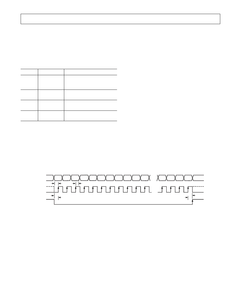
Control Register Serial Interface
The control register 3-wire interface timing requirements are
shown in Figure 7. Control data must be written into the device
one address at a time due to the noncontiguous address spacing
for the control registers. This requires eight bits of address data
followed by 24 bits of configuration data between each active
low period of SL for each address. The SL signal must be kept
high for at least one full SCK cycle between successive writes to
control registers.
System Register Serial Interface
There are seventeen 32-bit system registers that get accessed
sequentially at Address 0x14 beginning with Sys_Reg[0]. When
writing to the system registers, SDATA contains the 8-bit address
of 0x14, followed by Number Writes N[23:0], followed by the
Sys_Reg[31:0] data as shown in Figure 8. The system register
map is listed in Table II.
There are two options available when writing to the system
registers. The choice is automatically determined by the value of
the Number Writes N[23:0] word. If Number Writes N[23:0] =
0x000000, the device gets put into a mode where it expects all
17 Sys_Reg[31:0] data-words to be clocked in before SL is
asserted high. If the Number Writes N[23:0] is decoded as
some number N other than 0x000000, the device expects N
number of registers to be programmed where N is equal to the
value of Number Writes N[23:0]. For example, if Number
Writes N[23:0] = 0x000004, the device would expect data to be
provided for Sys_Reg[3:0]. In all cases, the system registers
would be written to begin with Sys_Reg[0], no matter what the
value of Number Writes N[23:0] is. Note that SL can be brought
high or low during access to system registers, as shown in Figure 8.
Mode_A and Mode_B Register Serial Interface
There are eight 32-bit Mode_A and eight 32-bit Mode_B regis-
ters that get accessed sequentially at Address 0x15 and Address
0x16, respectively. The Mode_A and Mode_B registers get
written to exactly as the system registers are. (See the descrip-
tion above.) The mode registers are listed in Tables III and IV.
Changing operation between Mode_A and Mode_B is done by
setting the 1-bit MODE register (Addr 0x0A). The desired
Mode_A (Addr 0x15) or Mode_B (Addr 0x16) data must be
programmed into the Mode_A or Mode_B registers before
changing the MODE bit.
SDATA
SCK
SL
A5
A6
D22
D21
D3
D2
D1
1. SDATA BITS ARE INTERNALLY LATCHED ON THE RISING EDGES OF SCK.
2. SYSTEM UPDATE OF LOADED REGISTERS OCCURS ON SL RISING EDGE.
3. THIS TIMING PATTERN MUST BE WRITTEN FOR EACH REGISTER WRITE WITH SL REMAINING HIGH FOR AT
LEAST ONE FULL SCK PERIOD BEFORE ASSERTING SL LOW AGAIN FOR THE NEXT REGISTER WRITE.
A7
A4
A3
A2
A1
A0
D23
....
....
D0
1
2
3
4
5
6
7
8
9
10
11
29
30
31
t
LH
32
t
DS
t
DH
t
LS
Figure 7. 3-Wire Serial Interface Timing for Control Registers
相關PDF資料 |
PDF描述 |
|---|---|
| AD9901 | Ultrahigh Speed Phase/Frequency Discriminator |
| AD9901KP | Ultrahigh Speed Phase/Frequency Discriminator |
| AD9901KQ | TVS Diode; Diode Type:Bidirectional TVS; Stand-Off Voltage, VRWM:30V; Breakdown Voltage, Vbr:33.3V; Package/Case:DO-214AB; Leaded Process Compatible:Yes; No. of Lines Protected Max:1; Peak Pulse Power PPK @ 10x1000uS:1500W RoHS Compliant: Yes |
| AD9910 | 1 GSPS, 14-Bit, 3.3 V CMOS Direct Digital Synthesizer |
| AD9910_07 | 1 GSPS, 14-Bit, 3.3 V CMOS Direct Digital Synthesizer |
相關代理商/技術參數 |
參數描述 |
|---|---|
| AD9899ARS-2 | 制造商:Analog Devices 功能描述: |
| AD9901 | 制造商:AD 制造商全稱:Analog Devices 功能描述:Ultrahigh Speed Phase/Frequency Discriminator |
| AD9901KP | 制造商:Analog Devices 功能描述:PLL Frequency Synthesizer Single 20-Pin PLCC 制造商:Rochester Electronics LLC 功能描述:IC VHF PHCOMP AD9901 IC - Bulk 制造商:Analog Devices 功能描述:IC DISCRIMINATOR |
| AD9901KP-REEL | 制造商:Analog Devices 功能描述:PLL Frequency Synthesizer Single 20-Pin PLCC T/R 制造商:Rochester Electronics LLC 功能描述:PHASE FREQ COMPARATOR IC - Tape and Reel |
| AD9901KPZ | 功能描述:IC PHS/FREQ DISCRIMINATOR 20PLCC RoHS:是 類別:集成電路 (IC) >> 時鐘/計時 - 時鐘發生器,PLL,頻率合成器 系列:- 標準包裝:2,000 系列:- 類型:PLL 頻率合成器 PLL:是 輸入:晶體 輸出:時鐘 電路數:1 比率 - 輸入:輸出:1:1 差分 - 輸入:輸出:無/無 頻率 - 最大:1GHz 除法器/乘法器:是/無 電源電壓:4.5 V ~ 5.5 V 工作溫度:-20°C ~ 85°C 安裝類型:表面貼裝 封裝/外殼:16-LSSOP(0.175",4.40mm 寬) 供應商設備封裝:16-SSOP 包裝:帶卷 (TR) 其它名稱:NJW1504V-TE1-NDNJW1504V-TE1TR |
發布緊急采購,3分鐘左右您將得到回復。