- 您現在的位置:買賣IC網 > PDF目錄382738 > Z550 Telecomm/Datacomm PDF資料下載
參數資料
| 型號: | Z550 |
| 元件分類: | 通信、網絡模塊及開發工具 |
| 英文描述: | Telecomm/Datacomm |
| 中文描述: | 電信/數據通信 |
| 文件頁數: | 14/30頁 |
| 文件大小: | 581K |
| 代理商: | Z550 |
第1頁第2頁第3頁第4頁第5頁第6頁第7頁第8頁第9頁第10頁第11頁第12頁第13頁當前第14頁第15頁第16頁第17頁第18頁第19頁第20頁第21頁第22頁第23頁第24頁第25頁第26頁第27頁第28頁第29頁第30頁
I
Z550 UART
I
––––––––––––––––––––––––––––––––––––––––––––––––––––––––––––––––––––––––––––––––––
14
Oki Semiconductor
Interrupt Enable Register
The Interrupt Enable Register (IER) is used to independently enable the four serial channel interrupts
which activate the interrupt (INTR) output. All interrupts are disabled by resetting IER(0) - IER(3) of the
Interrupt Enable Register to a logic “0”. Interrupts are enabled by setting the appropriate bits of the IER
high. Disabling the interrupt system inhibits the Interrupt Identification Register and the INTR output. All
other system functions operate in their normal manner, including the setting of the Line Status and
Modem Status Registers. The contents of the Interrupt Enable Register is described in the following table. .
Interrupt Enable Register Bits
Baud Rate Generator
The ACE serial channel contains a programmable Baud Rate Generator (BRG) that divides the clock (DC
to 3.1 MHz) by any divisor from 1 to 216-1. The output of the Baud Rate Generator is referred to as RCLK.
The frequency of RCLK 16x the data rate. The desired divisor is calculated by the following equation:
[divisor = clock
÷
(baud rate x 16)]. Two 8-bit divisor latch registers store the divisor in a 16-bit binary for-
mat. These Divisor Latch registers must be loaded during initialization. Upon loading ether of the Divisor
Latches, a 16-bit baud counter is immediately loaded. This prevents long counts on initial load. Setting
DLL = 1 and DLM = 0 selects a divisor = 1 (dividing by 1 gives maximum baud rate for a given input fre-
quency at the CLK input).
1. The exact time will be [(word length) x 7 - 2] x 8 + [(trigger level - number of characters) x 8 + 1] RCLKs.
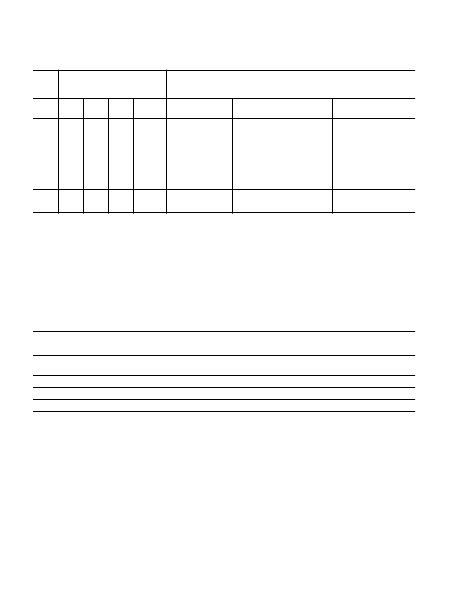
1
1
0
0
Second
Trigger Change
Level Indication
Minimum of one character in
the RCVR FIFO and no
character input or removed
during a time period
depending on how many
characters are in FIFO and
what the trigger level is set at
(3.5 to 4.5 character times
[1]
).
RBR read
0
0
1
0
Third
THRE
THRE
Read of IIR or THR write
0
0
0
0
Fourth
Modem Status
CTS, DSR, RI, or DCD
MSR read
IER Bit(s)
Bit Description
IER(0):
When programmed high (IER(0) = Logic “1”), ERBFI enables the Received Data Available Interrupt.
IER(1):
When programmed high (IER(1) = Logic “1”), ETBEI enables the Transmitter Holding Register Empty
Interrupt.
IER(2):
When programmed high (IER(2) = Logic “1”), ELSI enables the Receiver Line Status Interrupt.
IER(3):
When programmed high (IER(3) = Logic “1”), EDSSI enables the Modem Status Interrupt.
IER(4) - IER(7):
These four bits of the IER are logic “0”.
Interrupt Identification (IIR) Register Description
FIFO
Mode
Only
Interrupt Identification
Interrupt Set and Reset Functions
Bit 3
Bit 2
Bit 1
Bit 0
Priority
Level
Interrupt Flag
Interrupt Source
Interrupt Reset Control
相關PDF資料 |
PDF描述 |
|---|---|
| Z5904 | Leaded Cartridge Fuse; Current Rating:1A; Voltage Rating:250V; Fuse Terminals:Axial Lead; Fuse Type:Time Delay; Body Material:Glass; Diameter:4.5mm; Fuse Size/Group:5 x 15 mm; Leaded Process Compatible:No; Length:14.48mm |
| Z6000(MLBA2) | FUSE,FAST ACTING,3A,250VAC |
| Z6005 | 3A 250V SLO-BLO NR 5X20MM |
| Z6006 | TANK SPRAY WASH |
| Z6011 | PCB PROCESSOR 3 SYSTEM |
相關代理商/技術參數 |
參數描述 |
|---|---|
| Z550LA40A | 制造商:HVCA & CKE 功能描述:RADIAL LEAD MOV - LINE VOLTAGE - STANDARD ENERGY, 1500V, 50A, 180PF |
| Z550LA80A | 制造商:HVCA & CKE 功能描述:Varistor, MO; 910V; 6500A; 350pF |
| Z550MC10 | 制造商:OMRON AUTOMATION AND SAFETY 功能描述:Z550 SENSOR HEAD 制造商:OMRON Industrial Automation 功能描述:Z550 SENSOR HEAD |
| Z550-MC10 | 制造商:OMRON AUTOMATION AND SAFETY 功能描述:Z550 SENSOR HEAD 制造商:OMRON Industrial Automation 功能描述:Z550 SENSOR HEAD 制造商:OMRON INDUSTRIAL AUTOMATION 功能描述:Z550 Sensor Head |
| Z550MC15 | 制造商:OMRON AUTOMATION AND SAFETY 功能描述:Z550 SENSOR HEAD |
發布緊急采購,3分鐘左右您將得到回復。