- 您現在的位置:買賣IC網 > PDF目錄371053 > MC68HC916X1 (Motorola, Inc.) 16-Bit Modular Microcontroller(16位模塊化微控制器) PDF資料下載
參數資料
| 型號: | MC68HC916X1 |
| 廠商: | Motorola, Inc. |
| 英文描述: | 16-Bit Modular Microcontroller(16位模塊化微控制器) |
| 中文描述: | 16位微控制器模塊(16位模塊化微控制器) |
| 文件頁數: | 163/172頁 |
| 文件大小: | 1035K |
| 代理商: | MC68HC916X1 |
第1頁第2頁第3頁第4頁第5頁第6頁第7頁第8頁第9頁第10頁第11頁第12頁第13頁第14頁第15頁第16頁第17頁第18頁第19頁第20頁第21頁第22頁第23頁第24頁第25頁第26頁第27頁第28頁第29頁第30頁第31頁第32頁第33頁第34頁第35頁第36頁第37頁第38頁第39頁第40頁第41頁第42頁第43頁第44頁第45頁第46頁第47頁第48頁第49頁第50頁第51頁第52頁第53頁第54頁第55頁第56頁第57頁第58頁第59頁第60頁第61頁第62頁第63頁第64頁第65頁第66頁第67頁第68頁第69頁第70頁第71頁第72頁第73頁第74頁第75頁第76頁第77頁第78頁第79頁第80頁第81頁第82頁第83頁第84頁第85頁第86頁第87頁第88頁第89頁第90頁第91頁第92頁第93頁第94頁第95頁第96頁第97頁第98頁第99頁第100頁第101頁第102頁第103頁第104頁第105頁第106頁第107頁第108頁第109頁第110頁第111頁第112頁第113頁第114頁第115頁第116頁第117頁第118頁第119頁第120頁第121頁第122頁第123頁第124頁第125頁第126頁第127頁第128頁第129頁第130頁第131頁第132頁第133頁第134頁第135頁第136頁第137頁第138頁第139頁第140頁第141頁第142頁第143頁第144頁第145頁第146頁第147頁第148頁第149頁第150頁第151頁第152頁第153頁第154頁第155頁第156頁第157頁第158頁第159頁第160頁第161頁第162頁當前第163頁第164頁第165頁第166頁第167頁第168頁第169頁第170頁第171頁第172頁
MC68HC916X1
MC68HC916X1TS/D
MOTOROLA
163
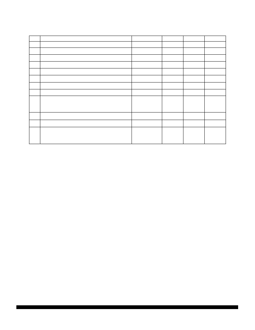
1. Below disruptive current conditions, a stressed channel will store the maximum conversion value for analog inputs
greater than V
RH
and the minimum conversion value for inputs less than V
RL
. This assumes that V
RH
≤
V
DDA
and
V
RL
≥
V
SSA
due to the presence of the sample amplifier. Other channels are not affected by non-disruptive con-
ditions
2. Input signals with large slew rates or high frequency noise components cannot be converted accurately. These
signals also interfere with conversion of other channels.
3. Exceeding limit may cause conversion error on stressed channels and on unstressed channels. Transitions within
the limit do not affect device reliability or cause permanent damage.
4. Input must be current limited to the value specified. To determine the value of the required current-limiting resistor,
calculate resistance values using positive and negative clamp values, then use the larger of the calculated values.
5. This parameter is periodically sampled rather than 100% tested.
6. Applies to single pin only.
7. The values of external system components can change the maximum input current value, and affect operation.
A voltage drop may occur across the external source impedances of the adjacent pins, impacting conversions on
these adjacent pins. The actual maximum may need to be determined by testing the complete design.
8. Current coupling is the ratio of the current induced from overvoltage (positive or negative, through an external
series coupling resistor), divided by the current induced on adjacent pins. A voltage drop may occur across the
external source impedances of the adjacent pins, impacting conversions on these adjacent pins.
Table 82 ADC Maximum Ratings
Num
1
Parameter
Symbol
V
DDA
V
DDI
V
RH
, V
RL
V
SSI
– V
SSA
V
DDI
– V
DDA
V
RH
– V
RL
V
RH
– V
DDA
V
RL
– V
SSA
Min
– 0.3
Max
6.5
Unit
V
Analog Supply
Internal Digital Supply, with reference to V
SSI
Reference Supply, with reference to V
SSI
V
SS
Differential Voltage
V
DD
Differential Voltage
V
REF
Differential Voltage
V
RH
to V
DDA
Differential Voltage
V
RL
to V
SSA
Differential Voltage
Disruptive Input Current
1
,
2
,
3
,
4
,
5
,
6
,
7
V
NEGCLAMP
–0.3V
V
POSCLAMP
8 V
2
– 0.3
6.5
V
3
– 0.3
6.5
V
4
– 0.1
0.1
V
5
– 6.5
6.5
V
6
– 6.5
6.5
V
7
– 6.5
6.5
V
8
– 6.5
6.5
V
9
I
NA
– 500
500
μ
A
10
Positive Overvoltage Current Coupling Ratio
1,
5,
6,
8
K
P
2000
—
—
11
Negative Overvoltage Current Coupling Ratio
1,
5,
6,
8
K
N
500
—
—
12
Maximum Input Current
3, 4, 6
V
NEGCLAMP
–0.3 V
V
POSCLAMP
8 V
I
MA
– 25
25
mA
相關PDF資料 |
PDF描述 |
|---|---|
| MC68HC9D60 | Advance Information - Rev 4.0 |
| MC68HC12D60 | Advance Information - Rev 4.0 |
| MC68HCL05C8A | 8-Bit Microcontroller Units (MCU).(8位微控制器) |
| MC68HSC05C8A | 8-Bit Microcontroller Units (MCU).(8位微控制器) |
| MC68HCP11 | 8-Bit Microcontrollers |
相關代理商/技術參數 |
參數描述 |
|---|---|
| MC68HC98LJ12CFU | 制造商:Rochester Electronics LLC 功能描述: 制造商:Freescale Semiconductor 功能描述: |
| MC68HC98LJ12CFUE | 功能描述:8位微控制器 -MCU 8 BIT MCU RoHS:否 制造商:Silicon Labs 核心:8051 處理器系列:C8051F39x 數據總線寬度:8 bit 最大時鐘頻率:50 MHz 程序存儲器大小:16 KB 數據 RAM 大小:1 KB 片上 ADC:Yes 工作電源電壓:1.8 V to 3.6 V 工作溫度范圍:- 40 C to + 105 C 封裝 / 箱體:QFN-20 安裝風格:SMD/SMT |
| MC68HC9S08RC60 L33R DIE | 制造商:Motorola Inc 功能描述: |
| MC68HCP11A1CFN3 | 功能描述:8位微控制器 -MCU 8-bit HCMOS single chip MCU RoHS:否 制造商:Silicon Labs 核心:8051 處理器系列:C8051F39x 數據總線寬度:8 bit 最大時鐘頻率:50 MHz 程序存儲器大小:16 KB 數據 RAM 大小:1 KB 片上 ADC:Yes 工作電源電壓:1.8 V to 3.6 V 工作溫度范圍:- 40 C to + 105 C 封裝 / 箱體:QFN-20 安裝風格:SMD/SMT |
| MC68HCP11A1FN | 制造商:MOTORALA 功能描述: |
發布緊急采購,3分鐘左右您將得到回復。