- 您現在的位置:買賣IC網 > PDF目錄373970 > AD9910BSVZ-REEL (ANALOG DEVICES INC) 1 GSPS, 14-Bit, 3.3 V CMOS Direct Digital Synthesizer PDF資料下載
參數資料
| 型號: | AD9910BSVZ-REEL |
| 廠商: | ANALOG DEVICES INC |
| 元件分類: | DAC |
| 英文描述: | 1 GSPS, 14-Bit, 3.3 V CMOS Direct Digital Synthesizer |
| 中文描述: | SERIAL, PARALLEL, WORD INPUT LOADING, 14-BIT DAC, PDSO100 |
| 封裝: | ROHS COMPLIANT, MS-026AED-HD, TQFP-100 |
| 文件頁數: | 26/60頁 |
| 文件大小: | 764K |
| 代理商: | AD9910BSVZ-REEL |
第1頁第2頁第3頁第4頁第5頁第6頁第7頁第8頁第9頁第10頁第11頁第12頁第13頁第14頁第15頁第16頁第17頁第18頁第19頁第20頁第21頁第22頁第23頁第24頁第25頁當前第26頁第27頁第28頁第29頁第30頁第31頁第32頁第33頁第34頁第35頁第36頁第37頁第38頁第39頁第40頁第41頁第42頁第43頁第44頁第45頁第46頁第47頁第48頁第49頁第50頁第51頁第52頁第53頁第54頁第55頁第56頁第57頁第58頁第59頁第60頁
AD9910
Rev. 0 | Page 26 of 60
PFD
CP
PLL_LOOP_FILTER
VCO
÷N
PLL OUT
PLL IN
AVDD
REFCLK PLL
2
R1
C1
C2
0
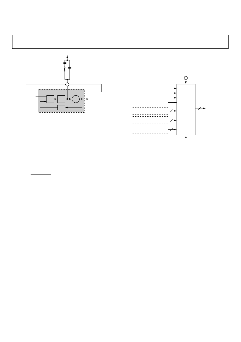
Figure 35. REFCLK PLL External Loop Filter
In the prevailing literature, this configuration yields a third-
order, Type II PLL. To calculate the loop filter component
values, begin with the feedback divider value (N), the gain of
the phase detector (K
D
), and the gain of the VCO (K
V
) based on
the programmed VCO SEL bit settings (see Table 1 for K
V
). The
loop filter component values depend on the desired open-loop
bandwidth (f
OL
) and phase margin (
φ
), as follows:
( )
+
=
K
K
Nf
π
R1
V
D
OL
sin
1
1
(4)
( )
)
2
(
f
2
tan
OL
V
D
N
K
K
C1
=
(5)
(
)
( )
( )
1
=
f
2
N
K
K
C2
OL
V
D
cos
sin
2
(6)
where:
K
D
is equal to the programmed value of I
CP
.
K
V
is taken from Table 1.
Ensure that proper units are used for the variables in Equation 4
through Equation 6. I
CP
must be in amps, not μA as appears in
Table 9; K
V
must be in Hz/V, not MHz/V as listed in Table 1; the
loop bandwidth (f
OL
) must be in Hz; the phase margin (φ) must
be in radians.
For example, suppose the PLL is programmed such that
I
CP
= 287 μA, K
V
= 625 MHz/V, and N = 25. If the desired loop
bandwidth and phase margin are 50 kHz and 45°, respectively,
then the loop filter component values are R1 = 52.85 Ω, C1 =
145.4 nF, and C2 = 30.11 nF.
PLL LOCK INDICATION
When the PLL is in use, the PLL_LOCK pin provides an active
high indication that the PLL has locked to the REFCLK input
signal. When the PLL is bypassed the PLL_LOCK pin defaults
to Logic 0.
OUTPUT SHIFT KEYING (OSK)
The OSK function (Figure 36) allows the user to control the
output signal amplitude of the DDS. Both a manual and an
automatic mode are available under program control. The
amplitude data generated by the OSK block has priority over
any other functional block that is programmed to deliver
amplitude data to the DDS. Hence, the OSK data source, when
enabled, overrides all other amplitude data sources.
0
OSK ENABLE
AMPLITUDE SCALE FACTOR
(ASF<15:2>)
AMPLITUDE RAMP RATE
(ASF<31:16>)
AMPLITUDE STEP SIZE
(ASF<1:0>)
MANUAL OSK EXTERNAL
AUTO OSK ENABLE
OSK
60
DDS CLOCK
TO DDS
AMPLITUDE
CONTROL
PARAMETER
LOAD ARR AT I/O_UPDATE
OSK
CONTROLLER
14
16
14
2
Figure 36. OSK Block Diagram
The operation of the OSK function is governed by four control
register bits, the external OSK pin, and the entire 32 bits of the
ASF register. The primary control for the OSK block is the OSK
enable bit. When the OSK function is disabled, the OSK input
controls are ignored and the internal clocks shut down.
When the OSK function is enabled, automatic and manual
operation is selected using the select auto OSK bit.
Manual OSK
In manual mode, output amplitude is varied by successive write
operations to the amplitude scale factor portion of the ASF
register. The rate at which amplitude changes can be applied to
the output signal is limited by the speed of the serial I/O port.
In manual mode, the OSK pin functionality depends on the
state of the manual OSK external bit. When the OSK pin is
Logic 0, the output amplitude is forced to zero; otherwise, the
output amplitude is set by the amplitude scale factor value.
Automatic OSK
In automatic mode, the OSK function automatically generates a
linear amplitude vs. time profile (or amplitude ramp). The
amplitude ramp is controlled via three parameters: the maximum
amplitude scale factor, the amplitude step size, and the time interval
between steps. The amplitude ramp parameters reside in the 32-bit
ASF register and are programmed via the serial I/O port. The time
interval between amplitude steps is set via the 16-bit amplitude
ramp rate portion of the ASF register (Bits<31:16>). The maximum
amplitude scale factor is set via the 14-bit amplitude scale factor in
the ASF register (Bits<15:2>). The amplitude step size is set via the
2-bit amplitude step size portion of the ASF register (Bits<1:0>).
Additionally, the direction of the ramp (positive or negative slope)
is controlled by the external OSK pin.
相關PDF資料 |
PDF描述 |
|---|---|
| AD9912 | 1 GSPS Direct Digital Synthesizer w/ 14-bit DAC |
| AD9913 | Low Power 250 MSPS 10-Bit DAC 1.8 V CMOS Direct Digital Synthesizer |
| AD9913BCPZ1 | Low Power 250 MSPS 10-Bit DAC 1.8 V CMOS Direct Digital Synthesizer |
| AD9913BCPZ-REEL71 | Low Power 250 MSPS 10-Bit DAC 1.8 V CMOS Direct Digital Synthesizer |
| AD9920A | 12-Bit CCD Signal Processor with V-Driver and Precision Timing Generator |
相關代理商/技術參數 |
參數描述 |
|---|---|
| AD9911 | 制造商:AD 制造商全稱:Analog Devices 功能描述:500 MSPS Direct Digital Synthesizer with 10-Bit DAC |
| AD9911/PCB | 制造商:Analog Devices 功能描述:500 MSPS DIRECT DGTL SYNTHESIZER W/ 10-BIT DAC AD9911/PCB - Bulk |
| AD9911/PCBZ | 功能描述:BOARD EVAL FOR AD9911 RoHS:是 類別:編程器,開發系統 >> 評估演示板和套件 系列:AgileRF™ 標準包裝:1 系列:PCI Express® (PCIe) 主要目的:接口,收發器,PCI Express 嵌入式:- 已用 IC / 零件:DS80PCI800 主要屬性:- 次要屬性:- 已供物品:板 |
| AD9911BCPZ | 功能描述:IC DDS 500MSPS DAC 10BIT 56LFCSP RoHS:是 類別:集成電路 (IC) >> 接口 - 直接數字合成 (DDS) 系列:- 產品變化通告:Product Discontinuance 27/Oct/2011 標準包裝:2,500 系列:- 分辨率(位):10 b 主 fclk:25MHz 調節字寬(位):32 b 電源電壓:2.97 V ~ 5.5 V 工作溫度:-40°C ~ 85°C 安裝類型:表面貼裝 封裝/外殼:16-TSSOP(0.173",4.40mm 寬) 供應商設備封裝:16-TSSOP 包裝:帶卷 (TR) |
| AD9911BCPZ-REEL7 | 功能描述:IC DDS 500MSPS DAC 10BIT 56LFCSP RoHS:是 類別:集成電路 (IC) >> 接口 - 直接數字合成 (DDS) 系列:- 產品變化通告:Product Discontinuance 27/Oct/2011 標準包裝:2,500 系列:- 分辨率(位):10 b 主 fclk:25MHz 調節字寬(位):32 b 電源電壓:2.97 V ~ 5.5 V 工作溫度:-40°C ~ 85°C 安裝類型:表面貼裝 封裝/外殼:16-TSSOP(0.173",4.40mm 寬) 供應商設備封裝:16-TSSOP 包裝:帶卷 (TR) |
發布緊急采購,3分鐘左右您將得到回復。