- 您現在的位置:買賣IC網 > PDF目錄373970 > AD9910BSVZ-REEL (ANALOG DEVICES INC) 1 GSPS, 14-Bit, 3.3 V CMOS Direct Digital Synthesizer PDF資料下載
參數資料
| 型號: | AD9910BSVZ-REEL |
| 廠商: | ANALOG DEVICES INC |
| 元件分類: | DAC |
| 英文描述: | 1 GSPS, 14-Bit, 3.3 V CMOS Direct Digital Synthesizer |
| 中文描述: | SERIAL, PARALLEL, WORD INPUT LOADING, 14-BIT DAC, PDSO100 |
| 封裝: | ROHS COMPLIANT, MS-026AED-HD, TQFP-100 |
| 文件頁數: | 44/60頁 |
| 文件大小: | 764K |
| 代理商: | AD9910BSVZ-REEL |
第1頁第2頁第3頁第4頁第5頁第6頁第7頁第8頁第9頁第10頁第11頁第12頁第13頁第14頁第15頁第16頁第17頁第18頁第19頁第20頁第21頁第22頁第23頁第24頁第25頁第26頁第27頁第28頁第29頁第30頁第31頁第32頁第33頁第34頁第35頁第36頁第37頁第38頁第39頁第40頁第41頁第42頁第43頁當前第44頁第45頁第46頁第47頁第48頁第49頁第50頁第51頁第52頁第53頁第54頁第55頁第56頁第57頁第58頁第59頁第60頁
AD9910
Rev. 0 | Page 44 of 60
LVDS
RECEIVER
PROGAMMABLE
DELAY
5
INTERNAL
CLOCKS
CLOCK
STATE
6
SYNC STATE
PRESET VALUE
SYNC PULSE
SYSCLK
SETUP AND HOLD
VALIDATION
4
D1
D2
Q1
Q2
LOAD
D6
D5
D4
D3
Q6
Q5
Q4
Q3
DELAYED SYNC-IN SIGNAL
SYNC
RECEIVER
DELAY
SYNC
RECEIVER
ENABLE
SYNC_SMP_ERR
SYNC_IN
7
8
12
RISING EDGE
DETECTOR
AND
STROBE
GENERATOR
SYNC
TIMING
VALIDATION
DISABLE
SYNC
VALIDATION
DELAY
0
CLOCK
GENERATOR
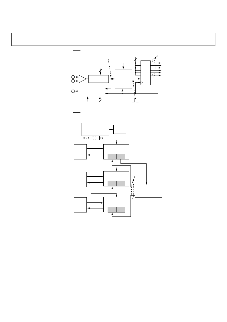
Figure 51. Sync Receiver Diagram
SYNC
IN
SYNC
OUT
REF_CLK
NUMBER 1
MASTER DEVICE
FPGA
DATA
FPGA
DATA
FPGA
DATA
EDGE
ALIGNED
AT REF_CLK
INPUTS.
EDGE
ALIGNED
AT SYN_IN
INPUTS.
P
SYNC
IN
SYNC
OUT
REF_CLK
NUMBER 2
P
SYNC
IN
SYNC
OUT
REF_CLK
NUMBER 3
P
(FOR EXAMPLE AD951x)
CLOCK DISTRIBUTION
AND
DELAY EQUALIZATION
SYNCHRONIZATION
DISTRIBUTION AND
DELAY EQUALIZATION
(FOR EXAMPLE AD951x)
0
CLOCK
SOURCE
Figure 52. Multichip Synchronization Example
The sync receiver accepts a periodic clock signal at the
SYNC_IN pins. This signal is assumed to originate from an
LVDS-compatible driver. The user can delay the SYNC_IN
signal in steps of ~150 ps by programming the 5-bit sync
receiver delay word in the multichip sync register. For the sake
of discussion, the signal at the output of the programmable
delay is referred to as the delayed sync-in signal.
The edge detection logic generates a sync pulse having a dura-
tion of one SYSCLK cycle with a repetition rate equal to the
frequency of the signal applied to the SYNC_IN pins. The sync
pulse is generated as a result of sampling the rising edge of the
delayed sync-in signal with the rising edge of the local SYSCLK.
The sync pulse is routed to the internal clock generator, which
behaves as a presettable counter clocked at the SYSCLK rate.
The sync pulse presets the counter to a predefined state
(programmable via the 6-bit sync state preset value word in the
multichip sync register). The predefined state is only active for a
single SYSCLK cycle, after which the clock generator resumes
cycling through its state sequence at the SYSCLK rate. This
unique state presetting mechanism gives the user the flexibility
to synchronize devices with specific relative clock state offsets
(by assigning a different sync state preset value word to each
device).
Multiple device synchronization is accomplished by providing
each AD9910 with a SYNC_IN signal that is edge aligned across
all the devices. If the SYNC_IN signal is edge aligned at all devices,
and all devices have the same sync receiver delay and sync state
preset value, then they all have matching clock states (that is, they
相關PDF資料 |
PDF描述 |
|---|---|
| AD9912 | 1 GSPS Direct Digital Synthesizer w/ 14-bit DAC |
| AD9913 | Low Power 250 MSPS 10-Bit DAC 1.8 V CMOS Direct Digital Synthesizer |
| AD9913BCPZ1 | Low Power 250 MSPS 10-Bit DAC 1.8 V CMOS Direct Digital Synthesizer |
| AD9913BCPZ-REEL71 | Low Power 250 MSPS 10-Bit DAC 1.8 V CMOS Direct Digital Synthesizer |
| AD9920A | 12-Bit CCD Signal Processor with V-Driver and Precision Timing Generator |
相關代理商/技術參數 |
參數描述 |
|---|---|
| AD9911 | 制造商:AD 制造商全稱:Analog Devices 功能描述:500 MSPS Direct Digital Synthesizer with 10-Bit DAC |
| AD9911/PCB | 制造商:Analog Devices 功能描述:500 MSPS DIRECT DGTL SYNTHESIZER W/ 10-BIT DAC AD9911/PCB - Bulk |
| AD9911/PCBZ | 功能描述:BOARD EVAL FOR AD9911 RoHS:是 類別:編程器,開發系統 >> 評估演示板和套件 系列:AgileRF™ 標準包裝:1 系列:PCI Express® (PCIe) 主要目的:接口,收發器,PCI Express 嵌入式:- 已用 IC / 零件:DS80PCI800 主要屬性:- 次要屬性:- 已供物品:板 |
| AD9911BCPZ | 功能描述:IC DDS 500MSPS DAC 10BIT 56LFCSP RoHS:是 類別:集成電路 (IC) >> 接口 - 直接數字合成 (DDS) 系列:- 產品變化通告:Product Discontinuance 27/Oct/2011 標準包裝:2,500 系列:- 分辨率(位):10 b 主 fclk:25MHz 調節字寬(位):32 b 電源電壓:2.97 V ~ 5.5 V 工作溫度:-40°C ~ 85°C 安裝類型:表面貼裝 封裝/外殼:16-TSSOP(0.173",4.40mm 寬) 供應商設備封裝:16-TSSOP 包裝:帶卷 (TR) |
| AD9911BCPZ-REEL7 | 功能描述:IC DDS 500MSPS DAC 10BIT 56LFCSP RoHS:是 類別:集成電路 (IC) >> 接口 - 直接數字合成 (DDS) 系列:- 產品變化通告:Product Discontinuance 27/Oct/2011 標準包裝:2,500 系列:- 分辨率(位):10 b 主 fclk:25MHz 調節字寬(位):32 b 電源電壓:2.97 V ~ 5.5 V 工作溫度:-40°C ~ 85°C 安裝類型:表面貼裝 封裝/外殼:16-TSSOP(0.173",4.40mm 寬) 供應商設備封裝:16-TSSOP 包裝:帶卷 (TR) |
發布緊急采購,3分鐘左右您將得到回復。