- 您現(xiàn)在的位置:買賣IC網(wǎng) > PDF目錄373970 > AD9910BSVZ-REEL (ANALOG DEVICES INC) 1 GSPS, 14-Bit, 3.3 V CMOS Direct Digital Synthesizer PDF資料下載
參數(shù)資料
| 型號: | AD9910BSVZ-REEL |
| 廠商: | ANALOG DEVICES INC |
| 元件分類: | DAC |
| 英文描述: | 1 GSPS, 14-Bit, 3.3 V CMOS Direct Digital Synthesizer |
| 中文描述: | SERIAL, PARALLEL, WORD INPUT LOADING, 14-BIT DAC, PDSO100 |
| 封裝: | ROHS COMPLIANT, MS-026AED-HD, TQFP-100 |
| 文件頁數(shù): | 34/60頁 |
| 文件大小: | 764K |
| 代理商: | AD9910BSVZ-REEL |
第1頁第2頁第3頁第4頁第5頁第6頁第7頁第8頁第9頁第10頁第11頁第12頁第13頁第14頁第15頁第16頁第17頁第18頁第19頁第20頁第21頁第22頁第23頁第24頁第25頁第26頁第27頁第28頁第29頁第30頁第31頁第32頁第33頁當前第34頁第35頁第36頁第37頁第38頁第39頁第40頁第41頁第42頁第43頁第44頁第45頁第46頁第47頁第48頁第49頁第50頁第51頁第52頁第53頁第54頁第55頁第56頁第57頁第58頁第59頁第60頁
AD9910
Note that two-level modulation can be accomplished by using
only one of the three profile pins to toggle between two
different parameter values. Likewise, four-level modulation can
be accomplished by using only two of the three profile pins.
There is no restriction on which profile pins are used.
Rev. 0 | Page 34 of 60
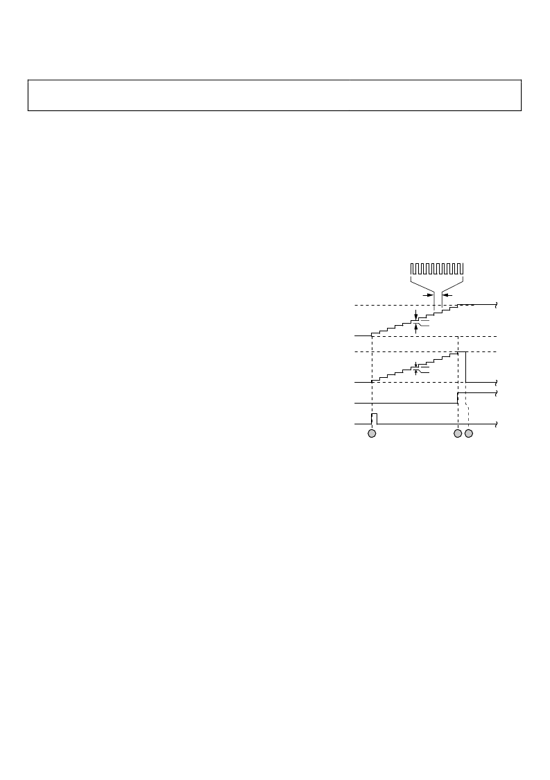
Ramp Up Timing Diagram
A graphic representation of the ramp up mode appears in
Figure 43, showing both normal and no-dwell operation.
The two upper traces show the progression of the RAM address
from the waveform start address to the waveform end address
for the selected profile. The address value advances by one with
each timeout of the timer internal to the state machine. The
timer period (Δt) is determined by the address ramp rate value
for the selected profile. The two upper traces are differentiated
by the state of the no-dwell high bit.
RAM Direct Switch Mode with Zero-Crossing
The zero-crossing function (enabled with the zero-crossing bit)
is a special feature that is only available in RAM direct switch
mode. The zero-crossing function is only valid if the RAM
playback destination bits specify phase as the DDS signal
control parameter.
0
WAVEFORM START ADDRESS
WAVEFORM END ADDRESS
WAVEFORM START ADDRESS
WAVEFORM END ADDRESS
1
M DDS CLOCK CYCLES
NO-DWELL
HIGH = 0
NO-DWELL
HIGH = 1
1
RAM ADDRESS
RAM ADDRESS
RAM_SWP_OVER
I/O_UPDATE
1
2
3
Δ
t
Enabling zero-crossing causes the DDS to delay the application
of a new phase value until such time as the DDS phase
accumulator rolls over from full scale to zero (the point at
which the DDS phase accumulator represents a phase angle that
is at the 360° to 0° transition point). This can be a very
beneficial feature when the DDS is programmed to generate a
sine wave (using the select DDS sine output bit), because the
zero-crossing point of phase for a sine wave corresponds with
the zero-crossing point of amplitude.
In the case of binary phase shift keying (BPSK), the zero-
crossing feature allows the AD9910 to perform the 180° phase
jumps associated with BPSK with only a minimal instantaneous
change in amplitude. This avoids the spectral splatter that
frequently accompanies BPSK modulation.
Although the intent of the zero-crossing feature is for use with
the DDS sine output enabled, it can be used with a cosine
output. In this case, the phase values extracted from RAM are
registered at the DDS when the output amplitude is at its peak
positive value.
Figure 43. Ramp Up Timing Diagram
The circled numbers in Figure 43 indicate specific events
explained as follows:
Event 1—An I/O update or profile change occurs. This event
initializes the state machine to the waveform start address and
sets the RAM_SWP_OVR pin to Logic 0.
RAM Ramp Up Mode
In ramp up mode, upon assertion of an I/O update or a change
of profile, the RAM begins operating as a waveform generator
using the parameters programmed into the selected RAM
profile register. Data is extracted from RAM over the specified
address range and at the specified rate contained in the wave-
form start address, waveform end address, and address ramp
rate values of the selected RAM profile. The data is delivered
to the specified DDS signal control parameter(s) based on the
RAM playback destination bits.
Event 2—The state machine reaches the waveform end address
value for the selected profile. The RAM_SWP_OVR pin
switches to Logic 1. This marks the end of the waveform
generation sequence for normal operation.
Event 3—The state machine switches to the waveform start
address. This marks the end of the waveform generation
sequence for no-dwell operation.
The internal state machine begins extracting data from the
RAM at the waveform start address and continues to extract
data until it reaches the waveform end address. Upon reaching
this address, it either remains at the waveform end address or
returns to the waveform start address as defined by the no-dwell
high bit. Then the state machine halts and the RAM_SWP_OVR
pin goes high.
Changing profiles resets the RAM_SWP_OVR pin to Logic 0,
automatically terminates the current waveform, and initiates the
newly selected waveform.
RAM Ramp Up Internal Profile Control Mode
Ramp up internal profile control mode is invoked via the four
internal profile control bits (rather than through the RAM
profile mode control bits in the RAM profile registers).
相關PDF資料 |
PDF描述 |
|---|---|
| AD9912 | 1 GSPS Direct Digital Synthesizer w/ 14-bit DAC |
| AD9913 | Low Power 250 MSPS 10-Bit DAC 1.8 V CMOS Direct Digital Synthesizer |
| AD9913BCPZ1 | Low Power 250 MSPS 10-Bit DAC 1.8 V CMOS Direct Digital Synthesizer |
| AD9913BCPZ-REEL71 | Low Power 250 MSPS 10-Bit DAC 1.8 V CMOS Direct Digital Synthesizer |
| AD9920A | 12-Bit CCD Signal Processor with V-Driver and Precision Timing Generator |
相關代理商/技術參數(shù) |
參數(shù)描述 |
|---|---|
| AD9911 | 制造商:AD 制造商全稱:Analog Devices 功能描述:500 MSPS Direct Digital Synthesizer with 10-Bit DAC |
| AD9911/PCB | 制造商:Analog Devices 功能描述:500 MSPS DIRECT DGTL SYNTHESIZER W/ 10-BIT DAC AD9911/PCB - Bulk |
| AD9911/PCBZ | 功能描述:BOARD EVAL FOR AD9911 RoHS:是 類別:編程器,開發(fā)系統(tǒng) >> 評估演示板和套件 系列:AgileRF™ 標準包裝:1 系列:PCI Express® (PCIe) 主要目的:接口,收發(fā)器,PCI Express 嵌入式:- 已用 IC / 零件:DS80PCI800 主要屬性:- 次要屬性:- 已供物品:板 |
| AD9911BCPZ | 功能描述:IC DDS 500MSPS DAC 10BIT 56LFCSP RoHS:是 類別:集成電路 (IC) >> 接口 - 直接數(shù)字合成 (DDS) 系列:- 產(chǎn)品變化通告:Product Discontinuance 27/Oct/2011 標準包裝:2,500 系列:- 分辨率(位):10 b 主 fclk:25MHz 調(diào)節(jié)字寬(位):32 b 電源電壓:2.97 V ~ 5.5 V 工作溫度:-40°C ~ 85°C 安裝類型:表面貼裝 封裝/外殼:16-TSSOP(0.173",4.40mm 寬) 供應商設備封裝:16-TSSOP 包裝:帶卷 (TR) |
| AD9911BCPZ-REEL7 | 功能描述:IC DDS 500MSPS DAC 10BIT 56LFCSP RoHS:是 類別:集成電路 (IC) >> 接口 - 直接數(shù)字合成 (DDS) 系列:- 產(chǎn)品變化通告:Product Discontinuance 27/Oct/2011 標準包裝:2,500 系列:- 分辨率(位):10 b 主 fclk:25MHz 調(diào)節(jié)字寬(位):32 b 電源電壓:2.97 V ~ 5.5 V 工作溫度:-40°C ~ 85°C 安裝類型:表面貼裝 封裝/外殼:16-TSSOP(0.173",4.40mm 寬) 供應商設備封裝:16-TSSOP 包裝:帶卷 (TR) |
發(fā)布緊急采購,3分鐘左右您將得到回復。