- 您現(xiàn)在的位置:買賣IC網(wǎng) > PDF目錄373970 > AD9923A (Analog Devices, Inc.) CCD Signal Processor with V-Driver and Precision Timing⑩ Generator PDF資料下載
參數(shù)資料
| 型號: | AD9923A |
| 廠商: | Analog Devices, Inc. |
| 英文描述: | CCD Signal Processor with V-Driver and Precision Timing⑩ Generator |
| 中文描述: | CCD信號處理器與V - Driver和精確定時⑩發(fā)生器 |
| 文件頁數(shù): | 55/88頁 |
| 文件大小: | 852K |
| 代理商: | AD9923A |
第1頁第2頁第3頁第4頁第5頁第6頁第7頁第8頁第9頁第10頁第11頁第12頁第13頁第14頁第15頁第16頁第17頁第18頁第19頁第20頁第21頁第22頁第23頁第24頁第25頁第26頁第27頁第28頁第29頁第30頁第31頁第32頁第33頁第34頁第35頁第36頁第37頁第38頁第39頁第40頁第41頁第42頁第43頁第44頁第45頁第46頁第47頁第48頁第49頁第50頁第51頁第52頁第53頁第54頁當前第55頁第56頁第57頁第58頁第59頁第60頁第61頁第62頁第63頁第64頁第65頁第66頁第67頁第68頁第69頁第70頁第71頁第72頁第73頁第74頁第75頁第76頁第77頁第78頁第79頁第80頁第81頁第82頁第83頁第84頁第85頁第86頁第87頁第88頁
AD9923A
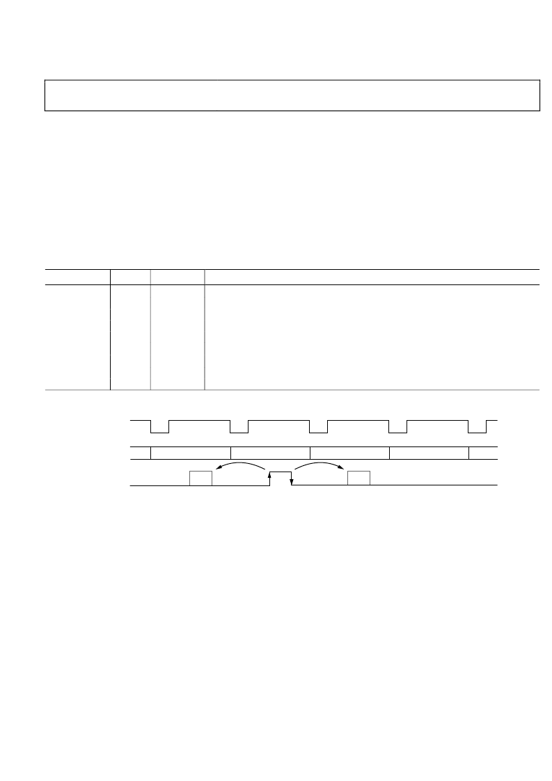
FG_TRIG OPERATION
The AD9923A contains one additional signal that can be used
in conjunction with shutter operation or general system
operation. The FG_TRIG signal is an internally generated pulse
that can be output on the SYNC pins for shutter or other system
functions. A unique feature of the FG_TRIG signal is that it is
output with respect to the MODE register field status.
Rev. 0 | Page 55 of 88
The FG_TRIG signal is generated using the SHUT1 start
polarity and toggle position registers, programmable with line
and pixel resolution. The field registers for SHUT1 are ignored
because the field placement of the FG_TRIG pulse is matched
to the field count specified by the MODE register operation.
The FG_TRIGEN register contains a three-bit value that specifies
which field count contains the FG_TRIG pulse. Figure 72 shows
how the FG_TRIG pulse is generated using these registers.
After the FG_TRIG signal is specified, it can be enabled using
Bit 3 of the FG_TRIGEN register. The FG_TRIG signal is
mapped to the SYNC output if the SYNC pin is configured as
an output (SYNCENABLE = 0).
Table 40. FG_TRIG Operation Registers
Register
SYNCENABLE
FG_TRIGEN
SHUT1POL
SHUT1_ON_LN
SHUT1_ON_PX
SHUT1_OFF_LN 0x76
SHUT1_OFF_PX
Address
0x12
0xF1
0x72
0x74
0x74
Bit Location
[0]
[3:0]
[1]
[11:0]
[25:13]
[11:0]
[25:13]
Description
0 = configures SYNC pin as an output. By default, the FG_TRIG signal is output on the SYNC pin.
1 = SYNC pin is an external synchronization input.
[2:0] selects the field count for the pulse based on the mode field counter.
[3] = 1 to enable FG_TRIG signal output.
[1] FG_TRIG start polarity.
FG_TRIG first toggle, line location.
FG_TRIG first toggle, pixel location.
FG_TRIG second toggle, line location.
FG_TRIG second toggle, pixel location.
0x76
VD
FG_TRIG PROGRAMMABLE SETTINGS:
1
ACTIVE POLARITY.
2
FIRST TOGGLE POSITION, LINE AND PIXEL LOCATION.
3
SECOND TOGGLE POSITION, LINE AND PIXEL LOCATION.
4
FIELD PLACEMENT BASED ON MODE REGISTER FIELD COUNT.
MODE REGISTER
FIELD COUNT
FG_TRIG
1
2
3
FIELD 0
FIELD 1
FIELD 2
FIELD 0
FIELD 1
4
4
0
Figure 72. FG_TRIG Signal Generation
相關(guān)PDF資料 |
PDF描述 |
|---|---|
| AD9923ABBCZ | CCD Signal Processor with V-Driver and Precision Timing⑩ Generator |
| AD9923ABBCZRL | CCD Signal Processor with V-Driver and Precision Timing⑩ Generator |
| AD9925BBCZRL | CCD Signal Processor with Vertical Driver and Precision Timing Generator |
| AD9925 | CCD Signal Processor with Vertical Driver and Precision Timing Generator |
| AD9925BBCZ | CCD Signal Processor with Vertical Driver and Precision Timing Generator |
相關(guān)代理商/技術(shù)參數(shù) |
參數(shù)描述 |
|---|---|
| AD9923ABBCZ | 功能描述:IC PROCESSOR CCD 12BIT 105CSPBGA RoHS:是 類別:集成電路 (IC) >> 接口 - 傳感器和探測器接口 系列:- 其它有關(guān)文件:Automotive Product Guide 產(chǎn)品培訓(xùn)模塊:Lead (SnPb) Finish for COTS Obsolescence Mitigation Program 標準包裝:74 系列:- 類型:觸控式傳感器 輸入類型:數(shù)字 輸出類型:數(shù)字 接口:JTAG,串行 電流 - 電源:100µA 安裝類型:表面貼裝 封裝/外殼:20-TSSOP(0.173",4.40mm 寬) 供應(yīng)商設(shè)備封裝:20-TSSOP 包裝:管件 |
| AD9923ABBCZRL | 功能描述:IC PROCESSOR CCD 12BIT 105CSPBGA RoHS:是 類別:集成電路 (IC) >> 接口 - 傳感器和探測器接口 系列:- 其它有關(guān)文件:Automotive Product Guide 產(chǎn)品培訓(xùn)模塊:Lead (SnPb) Finish for COTS Obsolescence Mitigation Program 標準包裝:74 系列:- 類型:觸控式傳感器 輸入類型:數(shù)字 輸出類型:數(shù)字 接口:JTAG,串行 電流 - 電源:100µA 安裝類型:表面貼裝 封裝/外殼:20-TSSOP(0.173",4.40mm 寬) 供應(yīng)商設(shè)備封裝:20-TSSOP 包裝:管件 |
| AD9923BBCZ | 制造商:Rochester Electronics LLC 功能描述:- Bulk 制造商:Analog Devices 功能描述: |
| AD9923BBCZRL | 制造商:Rochester Electronics LLC 功能描述: 制造商:Analog Devices 功能描述: |
| AD9924BBCZ | 制造商:Analog Devices 功能描述: |
發(fā)布緊急采購,3分鐘左右您將得到回復(fù)。