- 您現在的位置:買賣IC網 > PDF目錄373970 > AD9923A (Analog Devices, Inc.) CCD Signal Processor with V-Driver and Precision Timing⑩ Generator PDF資料下載
參數資料
| 型號: | AD9923A |
| 廠商: | Analog Devices, Inc. |
| 英文描述: | CCD Signal Processor with V-Driver and Precision Timing⑩ Generator |
| 中文描述: | CCD信號處理器與V - Driver和精確定時⑩發生器 |
| 文件頁數: | 59/88頁 |
| 文件大小: | 852K |
| 代理商: | AD9923A |
第1頁第2頁第3頁第4頁第5頁第6頁第7頁第8頁第9頁第10頁第11頁第12頁第13頁第14頁第15頁第16頁第17頁第18頁第19頁第20頁第21頁第22頁第23頁第24頁第25頁第26頁第27頁第28頁第29頁第30頁第31頁第32頁第33頁第34頁第35頁第36頁第37頁第38頁第39頁第40頁第41頁第42頁第43頁第44頁第45頁第46頁第47頁第48頁第49頁第50頁第51頁第52頁第53頁第54頁第55頁第56頁第57頁第58頁當前第59頁第60頁第61頁第62頁第63頁第64頁第65頁第66頁第67頁第68頁第69頁第70頁第71頁第72頁第73頁第74頁第75頁第76頁第77頁第78頁第79頁第80頁第81頁第82頁第83頁第84頁第85頁第86頁第87頁第88頁
AD9923A
Table 41. Power-Up Register Write Sequence
Register
Address
SW_RST
0x10
0x20 to 0xFFF
STANDBY
0x00
TEST3
0xEA
OSC_RST
0x16
TGCORE_RSTB
0x15
MASTER
0x20
OUTCONTROL
0x11
SYNCPOL
0x13
Rev. 0 | Page 59 of 88
Data
0x01
User defined
0x04
0x60
0x01
0x01
0x01
0x01
0x01
Description
Resets all registers to default values
Horizontal, vertical, shutter timing
Powers up the AFE
Set TEST3 register to required value
Resets crystal oscillator circuit
Resets internal timing core
Configures master mode
Enables all outputs after SYNC
SYNC active polarity (for software SYNC only)
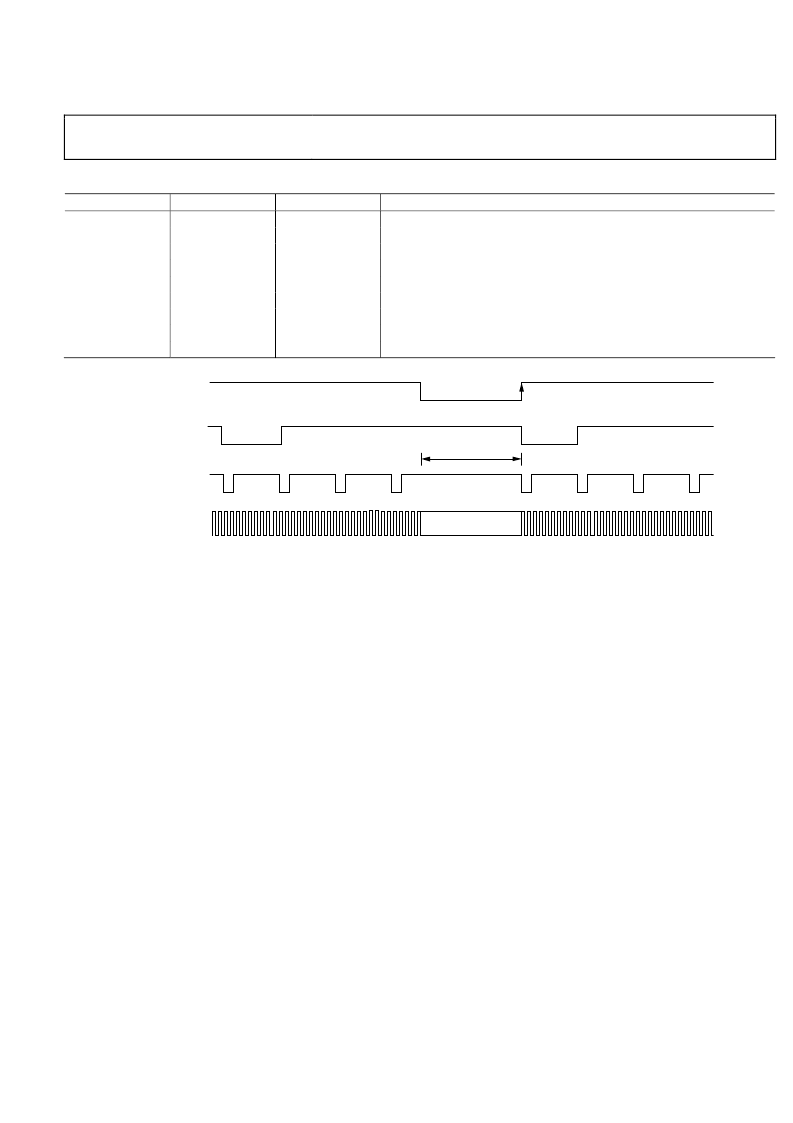
VD
HD
SUSPEND
SYNC
HL, H1 TO H4, RG,
XV1 TO XV13,
VSG1 TO VSG8, SUBCK
NOTES
1. THE SYNC RISING EDGE RESETS VD/HD AND COUNTERS TO 0.
2. SYNC POLARITY IS PROGRAMMABLE USING SYNCPOL REGISTER (ADDR 0x13).
3. DURING SYNC LOW, ALL INTERNAL COUNTERS ARE RESET AND VD/HD CAN BE SUSPENDED USING THE SYNCSUSPEND REGISTER (ADDR 0x14).
4. IF SYNCSUSPEND = 1, VERTICAL CLOCKS, H1 TO H4, AND RG ARE HELD AT THE SAME POLARITY SPECIFIED BY OUTCONTROL = LOW.
5. IF SYNCSUSPEND = 0, ALL CLOCK OUTPUTS CONTINUE TO OPERATE NORMALLY UNTIL SYNC RESET EDGE.
Figure 76. SYNC Timing to Synchronize AD9923A with External Timing
0
Generating Software Sync Without External Sync Signal
If an external sync pulse is not available, it is possible to generate
an internal sync pulse by writing to the SYNCPOL register
(Address 0x13). If the software SYNC option is used, the SYNC
input (Pin 35) should be low (VSS) during the power-up proce-
dure. After the power-up procedure is complete, the SYNC pin
can be used as an output by setting the SYNCENABLE register
low (Address 0x12).
After power-up, follow Step 1 to Step 9 of the procedure in the
Recommended Power-Up Sequence for Master Mode section.
For Step 10, instead of using the external sync pulse, write 1 to
the SYNCPOL register to generate an internal sync pulse and
begin the timing operation.
SYNC During Master Mode Operation
The SYNC input can be used anytime during master mode
operation to synchronize the AD9923A counters with external
timing, as shown in Figure 76.
To suspend operation of the digital outputs during the SYNC
operation, set the SYNCSUSPEND register (Address 0x14) to 1. If
SYNCSUSPEND = 1, the polarities of the outputs are held at the
same state as when OUTCONTROL = low, as shown in Table 42
and Table 43.
Power-Up and Synchronization in Slave Mode
The power-up procedure for slave mode operation is the same
as the procedure described for master mode operation, with
two exceptions:
Eliminate Step 8. Do not configure the part for master
mode timing.
No sync pulse is required in slave mode. Substitute Step 10
with starting the external VD and HD signals. This
synchronizes the part, allows the register updates, and
starts the timing operation.
Note that DCLK does not begin to transition until Step 7 is
complete.
When the AD9923A is in slave mode, the VD/HD inputs
synchronize the internal counters. After a falling edge of VD,
there is a latency of 34 master clock edges (CLI) after the falling
edge of HD until the internal H-counter is reset. The reset
operation is shown in Figure 77.
Note that if SHDLOC is set so that the 3 ns minimum delay
between the rising edge of SLI and the falling edge of the
internal SHD signal is not met, the internal H-counter can reset
after only 33 master clock edges (CLI).
相關PDF資料 |
PDF描述 |
|---|---|
| AD9923ABBCZ | CCD Signal Processor with V-Driver and Precision Timing⑩ Generator |
| AD9923ABBCZRL | CCD Signal Processor with V-Driver and Precision Timing⑩ Generator |
| AD9925BBCZRL | CCD Signal Processor with Vertical Driver and Precision Timing Generator |
| AD9925 | CCD Signal Processor with Vertical Driver and Precision Timing Generator |
| AD9925BBCZ | CCD Signal Processor with Vertical Driver and Precision Timing Generator |
相關代理商/技術參數 |
參數描述 |
|---|---|
| AD9923ABBCZ | 功能描述:IC PROCESSOR CCD 12BIT 105CSPBGA RoHS:是 類別:集成電路 (IC) >> 接口 - 傳感器和探測器接口 系列:- 其它有關文件:Automotive Product Guide 產品培訓模塊:Lead (SnPb) Finish for COTS Obsolescence Mitigation Program 標準包裝:74 系列:- 類型:觸控式傳感器 輸入類型:數字 輸出類型:數字 接口:JTAG,串行 電流 - 電源:100µA 安裝類型:表面貼裝 封裝/外殼:20-TSSOP(0.173",4.40mm 寬) 供應商設備封裝:20-TSSOP 包裝:管件 |
| AD9923ABBCZRL | 功能描述:IC PROCESSOR CCD 12BIT 105CSPBGA RoHS:是 類別:集成電路 (IC) >> 接口 - 傳感器和探測器接口 系列:- 其它有關文件:Automotive Product Guide 產品培訓模塊:Lead (SnPb) Finish for COTS Obsolescence Mitigation Program 標準包裝:74 系列:- 類型:觸控式傳感器 輸入類型:數字 輸出類型:數字 接口:JTAG,串行 電流 - 電源:100µA 安裝類型:表面貼裝 封裝/外殼:20-TSSOP(0.173",4.40mm 寬) 供應商設備封裝:20-TSSOP 包裝:管件 |
| AD9923BBCZ | 制造商:Rochester Electronics LLC 功能描述:- Bulk 制造商:Analog Devices 功能描述: |
| AD9923BBCZRL | 制造商:Rochester Electronics LLC 功能描述: 制造商:Analog Devices 功能描述: |
| AD9924BBCZ | 制造商:Analog Devices 功能描述: |
發布緊急采購,3分鐘左右您將得到回復。