- 您現(xiàn)在的位置:買賣IC網(wǎng) > PDF目錄373970 > AD9923ABBCZRL (ANALOG DEVICES INC) CCD Signal Processor with V-Driver and Precision Timing⑩ Generator PDF資料下載
參數(shù)資料
| 型號: | AD9923ABBCZRL |
| 廠商: | ANALOG DEVICES INC |
| 元件分類: | 消費家電 |
| 英文描述: | CCD Signal Processor with V-Driver and Precision Timing⑩ Generator |
| 中文描述: | SPECIALTY CONSUMER CIRCUIT, PBGA105 |
| 封裝: | 8 X 8 MM, 0.65 MM PITCH, ROHS COMPLIANT, MO-225, CSPBGA-105 |
| 文件頁數(shù): | 24/88頁 |
| 文件大小: | 852K |
| 代理商: | AD9923ABBCZRL |
第1頁第2頁第3頁第4頁第5頁第6頁第7頁第8頁第9頁第10頁第11頁第12頁第13頁第14頁第15頁第16頁第17頁第18頁第19頁第20頁第21頁第22頁第23頁當(dāng)前第24頁第25頁第26頁第27頁第28頁第29頁第30頁第31頁第32頁第33頁第34頁第35頁第36頁第37頁第38頁第39頁第40頁第41頁第42頁第43頁第44頁第45頁第46頁第47頁第48頁第49頁第50頁第51頁第52頁第53頁第54頁第55頁第56頁第57頁第58頁第59頁第60頁第61頁第62頁第63頁第64頁第65頁第66頁第67頁第68頁第69頁第70頁第71頁第72頁第73頁第74頁第75頁第76頁第77頁第78頁第79頁第80頁第81頁第82頁第83頁第84頁第85頁第86頁第87頁第88頁
AD9923A
Increasing H-Clock Width During HBLK
The AD9923A allows the H1 to H4 pulse width to be increased
during the HBLK interval. The H-clock pulse width can in-
crease by reducing the H-clock frequency (see Table 13).
Rev. 0 | Page 24 of 88
The HBLKWIDTH register (Register 0x35, Bits[6:4]) is a 3-bit
register that allows the H-clock frequency to be reduced by 1/2,
1/4, 1/6, 1/8, 1/10, 1/12, or 1/14. The reduced frequency only
occurs for H1 to H4 pulses that are located within the HBLK area.
Horizontal Timing Sequence Example
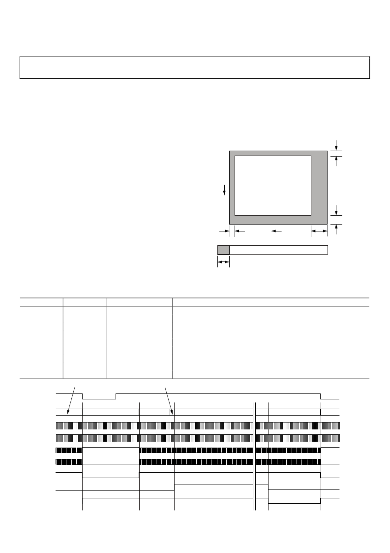
Figure 33 shows an example of a CCD layout. The horizontal
register contains 28 dummy pixels that occur on each line
clocked from the CCD. In the vertical direction, there are 10
optical black (OB) lines at the front of the readout and two at
the back of the readout. The horizontal direction has four OB
pixels in the front and 48 OB pixels in the back.
Figure 34 shows the basic sequence layout to use during the
effective pixel readout. The 48 OB pixels at the end of each line
are used for CLPOB signals. PBLK is optional and it is often
used to blank the digital outputs during the noneffective CCD
pixels. HBLK is used during the vertical shift interval.
The HBLK, CLPOB, and PBLK parameters are programmed in
the V-sequence registers. More elaborate clamping schemes can
be used, such as adding a separate sequence to clamp during the
entire line of OB pixels. This requires configuring a separate
V-sequence for reading the OB lines.
The CLPMASKSTART and CLPMASKEND registers can be used
to disable the CLPOB on a few lines without affecting the setup of
the clamp sequences.
HORIZONTAL CCD REGISTER
EFFECTIVE IMAGE AREA
28 DUMMY PIXELS
48 OB PIXELS
4 OB PIXELS
10 VERTICAL
OB LINES
2 VERTICAL
OB LINES
V
H
0
Figure 33. CCD Configuration Example
Table 13. HBLK Width Register
Register
HBLKWIDTH
Length (Bits)
3
Range
1× to 1/14× pixel rate
Description
Controls H1 to H4 width during HBLK as a fraction of pixel rate
0: same frequency as the pixel rate
1: 1/2 pixel frequency, that is, doubles the H1 to H4 pulse width
2: 1/4 pixel frequency
3: 1/6 pixel frequency
4: 1/8 pixel frequency
5: 1/10 pixel frequency
6: 1/12 pixel frequency
7: 1/14 pixel frequency
VERTICAL SHIFT
VERT. SHIFT
CCDIN
SHP
SHD
HL/H1/H3
H2/H4
HBLK
PBLK
CLPOB
OPTICAL BLACK
DUMMY
EFFECTIVE PIXELS
OPTICAL BLACK
OPTICAL BLACK
HD
0
Figure 34. Horizontal Sequence Example
相關(guān)PDF資料 |
PDF描述 |
|---|---|
| AD9925BBCZRL | CCD Signal Processor with Vertical Driver and Precision Timing Generator |
| AD9925 | CCD Signal Processor with Vertical Driver and Precision Timing Generator |
| AD9925BBCZ | CCD Signal Processor with Vertical Driver and Precision Timing Generator |
| AD9927 | 14-Bit CCD Signal Processor with V-Driver and Precision TimingTM Generator |
| AD9927BBCZ | 14-Bit CCD Signal Processor with V-Driver and Precision TimingTM Generator |
相關(guān)代理商/技術(shù)參數(shù) |
參數(shù)描述 |
|---|---|
| AD9923BBCZ | 制造商:Rochester Electronics LLC 功能描述:- Bulk 制造商:Analog Devices 功能描述: |
| AD9923BBCZRL | 制造商:Rochester Electronics LLC 功能描述: 制造商:Analog Devices 功能描述: |
| AD9924BBCZ | 制造商:Analog Devices 功能描述: |
| AD9924BBCZRL | 制造商:Rochester Electronics LLC 功能描述:- Bulk |
| AD9925 | 制造商:AD 制造商全稱:Analog Devices 功能描述:CCD Signal Processor with Vertical Driver and Precision Timing Generator |
發(fā)布緊急采購,3分鐘左右您將得到回復(fù)。