- 您現在的位置:買賣IC網 > PDF目錄373970 > AD9923ABBCZRL (ANALOG DEVICES INC) CCD Signal Processor with V-Driver and Precision Timing⑩ Generator PDF資料下載
參數資料
| 型號: | AD9923ABBCZRL |
| 廠商: | ANALOG DEVICES INC |
| 元件分類: | 消費家電 |
| 英文描述: | CCD Signal Processor with V-Driver and Precision Timing⑩ Generator |
| 中文描述: | SPECIALTY CONSUMER CIRCUIT, PBGA105 |
| 封裝: | 8 X 8 MM, 0.65 MM PITCH, ROHS COMPLIANT, MO-225, CSPBGA-105 |
| 文件頁數: | 68/88頁 |
| 文件大小: | 852K |
| 代理商: | AD9923ABBCZRL |
第1頁第2頁第3頁第4頁第5頁第6頁第7頁第8頁第9頁第10頁第11頁第12頁第13頁第14頁第15頁第16頁第17頁第18頁第19頁第20頁第21頁第22頁第23頁第24頁第25頁第26頁第27頁第28頁第29頁第30頁第31頁第32頁第33頁第34頁第35頁第36頁第37頁第38頁第39頁第40頁第41頁第42頁第43頁第44頁第45頁第46頁第47頁第48頁第49頁第50頁第51頁第52頁第53頁第54頁第55頁第56頁第57頁第58頁第59頁第60頁第61頁第62頁第63頁第64頁第65頁第66頁第67頁當前第68頁第69頁第70頁第71頁第72頁第73頁第74頁第75頁第76頁第77頁第78頁第79頁第80頁第81頁第82頁第83頁第84頁第85頁第86頁第87頁第88頁
AD9923A
UPDATING NEW REGISTER VALUES
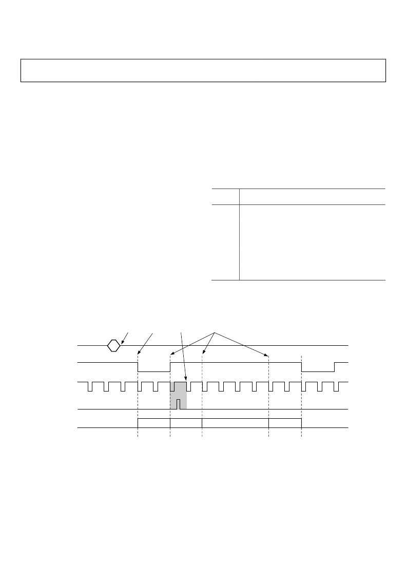
The AD9923A internal registers are updated at different times,
depending on the particular register. Table 44 summarizes the
four types of register updates. The register listing (Table 45
through Table 57) also contain a column with update type to
identify when each register is updated:
Rev. 0 | Page 68 of 88
SCK Updated
—Some registers are updated when the 28
th
data bit (D27) is written. These registers are used for
functions, such as power-up and reset, that do not require
gating with the next VD boundary.
VD Updated
—Many of the registers are updated at the
next VD falling edge. By updating these values at the next
VD edge, the current field is not corrupted, and the new
register values are applied to the next field. The VD update
can be further delayed, past the VD falling edge, by using
the UPDATE register (Address 0x18). This delays the
VD-updated register updates to any desired HD line in the
field. Note that the field registers are not affected by the
UPDATE register.
SG Updated
—A few shutter registers are updated at the
HD falling edge at the end of an SG active line. These
registers control the SUBCK signal; therefore, the SUBCK
output is not updated until the SG line is complete.
SCP Updated
—All V-pattern and V-sequence registers are
updated at the next SCP where they will be used. For
example, in Figure 88, this field has selected Region 1 to
use V-Sequence 3 for the vertical outputs; therefore, a write
to a V-Sequence 3 or V-pattern group register, which is
referenced by V-Sequence 3, is updated at SCP 1. If there
are multiple writes to the same register, only the last one
before SCP1 is updated. Likewise, a register write to a
V-Sequence 5 register is updated at SCP 2, and a register
write to a V-Sequence 8 register is updated at SCP 3.
Table 44. Register Update Locations
Update
Type
Description
SCK
Register is immediately updated when the 28
th
data
bit (D27) is written.
VD
Register is updated at the VD falling edge. VD
updated registers can be delayed further by using the
UPDATE register at Address 0x18. Field registers are
not affected by the UPDATE register.
SG
Register is updated at the HD falling edge at the end
of the SG active line.
SCP
Register is updated at the next SCP when the register
is used.
VD
REGION 0
HD
SCP 1
SCP 2
SCP 3
REGION 1
REGION 2
REGION 3
VSG
SGLINE
SCP 0
SERIAL
WRITE
SCK
UPDATED
SCP 0
VD
UPDATED
SG
UPDATED
SCP
UPDATED
V1A TO V10
USE VSEQ2
USE VSEQ3
USE VSEQ5
USE VSEQ8
0
Figure 88. Register Update Locations (See Table 44 for Definitions)
相關PDF資料 |
PDF描述 |
|---|---|
| AD9925BBCZRL | CCD Signal Processor with Vertical Driver and Precision Timing Generator |
| AD9925 | CCD Signal Processor with Vertical Driver and Precision Timing Generator |
| AD9925BBCZ | CCD Signal Processor with Vertical Driver and Precision Timing Generator |
| AD9927 | 14-Bit CCD Signal Processor with V-Driver and Precision TimingTM Generator |
| AD9927BBCZ | 14-Bit CCD Signal Processor with V-Driver and Precision TimingTM Generator |
相關代理商/技術參數 |
參數描述 |
|---|---|
| AD9923BBCZ | 制造商:Rochester Electronics LLC 功能描述:- Bulk 制造商:Analog Devices 功能描述: |
| AD9923BBCZRL | 制造商:Rochester Electronics LLC 功能描述: 制造商:Analog Devices 功能描述: |
| AD9924BBCZ | 制造商:Analog Devices 功能描述: |
| AD9924BBCZRL | 制造商:Rochester Electronics LLC 功能描述:- Bulk |
| AD9925 | 制造商:AD 制造商全稱:Analog Devices 功能描述:CCD Signal Processor with Vertical Driver and Precision Timing Generator |
發布緊急采購,3分鐘左右您將得到回復。