- 您現(xiàn)在的位置:買賣IC網(wǎng) > PDF目錄373970 > AD9923ABBCZRL (ANALOG DEVICES INC) CCD Signal Processor with V-Driver and Precision Timing⑩ Generator PDF資料下載
參數(shù)資料
| 型號: | AD9923ABBCZRL |
| 廠商: | ANALOG DEVICES INC |
| 元件分類: | 消費家電 |
| 英文描述: | CCD Signal Processor with V-Driver and Precision Timing⑩ Generator |
| 中文描述: | SPECIALTY CONSUMER CIRCUIT, PBGA105 |
| 封裝: | 8 X 8 MM, 0.65 MM PITCH, ROHS COMPLIANT, MO-225, CSPBGA-105 |
| 文件頁數(shù): | 37/88頁 |
| 文件大小: | 852K |
| 代理商: | AD9923ABBCZRL |
第1頁第2頁第3頁第4頁第5頁第6頁第7頁第8頁第9頁第10頁第11頁第12頁第13頁第14頁第15頁第16頁第17頁第18頁第19頁第20頁第21頁第22頁第23頁第24頁第25頁第26頁第27頁第28頁第29頁第30頁第31頁第32頁第33頁第34頁第35頁第36頁當(dāng)前第37頁第38頁第39頁第40頁第41頁第42頁第43頁第44頁第45頁第46頁第47頁第48頁第49頁第50頁第51頁第52頁第53頁第54頁第55頁第56頁第57頁第58頁第59頁第60頁第61頁第62頁第63頁第64頁第65頁第66頁第67頁第68頁第69頁第70頁第71頁第72頁第73頁第74頁第75頁第76頁第77頁第78頁第79頁第80頁第81頁第82頁第83頁第84頁第85頁第86頁第87頁第88頁
AD9923A
Vertical Sensor Gate (Shift Gate) Patterns
In an interline CCD, the vertical sensor gates (VSG) are used to
transfer the pixel charges from the light sensitive image area
into the light shielded vertical registers. From the light shielded
vertical registers, the image is then read line-by-line using the
XV1 to XV13 vertical transfer pulses in conjunction with the
high speed horizontal clocks.
Rev. 0 | Page 37 of 88
Table 19 summarizes the VSG pattern registers. The AD9923A
has eight VSG outputs, VSG1 to VSG8. Each output can be
assigned to one of eight programmed patterns by using the
SGPATSEL register. Each pattern is generated in a similar
manner as the V-pattern groups, with a programmable start
polarity (SGPOL), first toggle position (SGTOG1), and second
toggle position (SGTOG2). The active line where the VSG1 to
VSG8 pulses occur is programmable using the SGACTLINE1
and SGACTLINE2 registers. Additionally, any of the VSG1 to
VSG8 pulses can be individually disabled using the SGMASK
register. The individual masking allows all SG patterns to be
preprogrammed, and the appropriate pulses for each field can
be separately enabled. For maximum flexibility, the SGPATSEL,
SGMASK, and SGACTLINE registers are separately programmable
for each field. More detail is given in the Complete Field:
Combining V-Sequences section.
Additionally, there is the SGMASK_BYP register (Address 0x59)
that overrides SG masking in the field registers. The SGMASK_BYP
register allows sensor gate masking to be changed without
modifying the field register values. The SGMASK_BYP register
is SCK updated; therefore, the new SG-masking values update
immediately.
Table 19. VSG Pattern Registers
1
Register
SGPOL
SGTOG1
Length
(Bits)
1
13
Range
High/low
0 to 8191 pixel
location
0 to 8191 pixel
location
High/low for
each VSG
0 or 1
Description
Sensor gate starting polarity for SG patterns 0 to 7.
First toggle position for SG patterns 0 to 7.
SGTOG2
13
Second toggle position for SG patterns 0 to 7.
SGMASK_BYP
8
SGMASK Bypass. This register overrides the SGMASK values in each field register. One bit
for each output, where Bit[0] is for VSG1 output and Bit 7 is for VSG8 output.
0 = active.
1 = mask output.
1: enables SGMASK bypass.
SGMASK_BYP_EN
1
See field registers in Table 16.
1
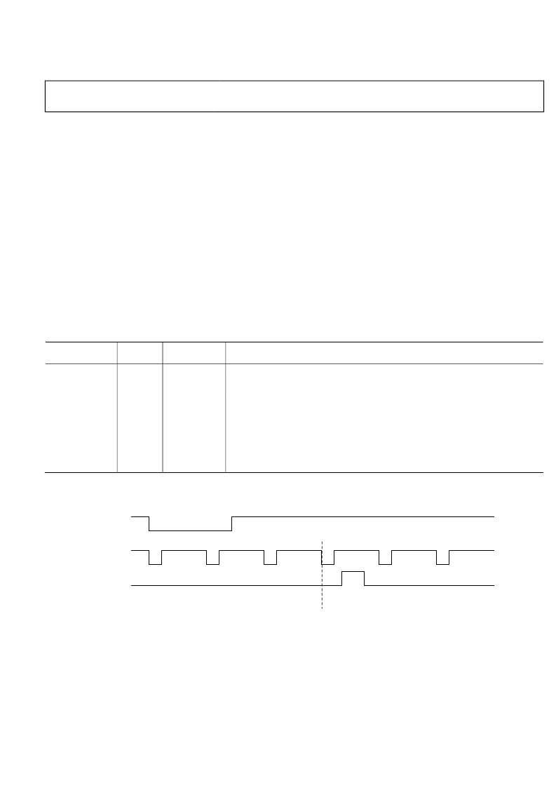
VD
HD
PROGRAMMABLE SETTINGS FOR EACH PATTERN:
1
START POLARITY OF PULSE.
2
FIRST TOGGLE POSITION.
3
SECOND TOGGLE POSITION.
4
ACTIVE LINE FOR VSG PULSES WITHIN THE FIELD (PROGRAMMABLE IN THE FIELD REGISTER, NOT FOR EACH PATTERN).
Figure 50. Vertical Sensor Gate Pulse Placement
VSG PATTERNS
4
1
2
3
0
相關(guān)PDF資料 |
PDF描述 |
|---|---|
| AD9925BBCZRL | CCD Signal Processor with Vertical Driver and Precision Timing Generator |
| AD9925 | CCD Signal Processor with Vertical Driver and Precision Timing Generator |
| AD9925BBCZ | CCD Signal Processor with Vertical Driver and Precision Timing Generator |
| AD9927 | 14-Bit CCD Signal Processor with V-Driver and Precision TimingTM Generator |
| AD9927BBCZ | 14-Bit CCD Signal Processor with V-Driver and Precision TimingTM Generator |
相關(guān)代理商/技術(shù)參數(shù) |
參數(shù)描述 |
|---|---|
| AD9923BBCZ | 制造商:Rochester Electronics LLC 功能描述:- Bulk 制造商:Analog Devices 功能描述: |
| AD9923BBCZRL | 制造商:Rochester Electronics LLC 功能描述: 制造商:Analog Devices 功能描述: |
| AD9924BBCZ | 制造商:Analog Devices 功能描述: |
| AD9924BBCZRL | 制造商:Rochester Electronics LLC 功能描述:- Bulk |
| AD9925 | 制造商:AD 制造商全稱:Analog Devices 功能描述:CCD Signal Processor with Vertical Driver and Precision Timing Generator |
發(fā)布緊急采購,3分鐘左右您將得到回復(fù)。