- 您現在的位置:買賣IC網 > PDF目錄371046 > MC68B912B32 (Motorola, Inc.) 2.5V 100ppm/Degrees C, 50uA in SOT23-3 Series (Bandgap) Voltage Reference 3-SOT-23 -40 to 125 PDF資料下載
參數資料
| 型號: | MC68B912B32 |
| 廠商: | Motorola, Inc. |
| 英文描述: | 2.5V 100ppm/Degrees C, 50uA in SOT23-3 Series (Bandgap) Voltage Reference 3-SOT-23 -40 to 125 |
| 中文描述: | 16位微控制器 |
| 文件頁數: | 113/128頁 |
| 文件大小: | 748K |
| 代理商: | MC68B912B32 |
第1頁第2頁第3頁第4頁第5頁第6頁第7頁第8頁第9頁第10頁第11頁第12頁第13頁第14頁第15頁第16頁第17頁第18頁第19頁第20頁第21頁第22頁第23頁第24頁第25頁第26頁第27頁第28頁第29頁第30頁第31頁第32頁第33頁第34頁第35頁第36頁第37頁第38頁第39頁第40頁第41頁第42頁第43頁第44頁第45頁第46頁第47頁第48頁第49頁第50頁第51頁第52頁第53頁第54頁第55頁第56頁第57頁第58頁第59頁第60頁第61頁第62頁第63頁第64頁第65頁第66頁第67頁第68頁第69頁第70頁第71頁第72頁第73頁第74頁第75頁第76頁第77頁第78頁第79頁第80頁第81頁第82頁第83頁第84頁第85頁第86頁第87頁第88頁第89頁第90頁第91頁第92頁第93頁第94頁第95頁第96頁第97頁第98頁第99頁第100頁第101頁第102頁第103頁第104頁第105頁第106頁第107頁第108頁第109頁第110頁第111頁第112頁當前第113頁第114頁第115頁第116頁第117頁第118頁第119頁第120頁第121頁第122頁第123頁第124頁第125頁第126頁第127頁第128頁
MC68HC912B32
MC68HC912B32TS/D
MOTOROLA
113
The ATD status registers contain the flags indicating the completion of ATD conversions.
Normally, it is read-only. In special mode, the SCF bit and the CCF bits may also be written.
SCF — Sequence Complete Flag
This bit is set at the end of the conversion sequence when in the single conversion sequence mode
(SCAN = 0 in ATDCTL5) and is set at the end of the first conversion sequence when in the continuous
conversion mode (SCAN = 1 in ATDCTL5). When AFFC = 0, SCF is cleared when a write is performed
to ATDCTL5 to initiate a new conversion sequence. When AFFC = 1, SCF is cleared after the first result
register is read.
CC[2:0] — Conversion Counter for Current Sequence of Four or Eight Conversions
This 3-bit value reflects the contents of the conversion counter pointer in a four or eight count sequence.
This value also reflects which result register will be written next, indicating which channel is currently
being converted.
CCF[7:0] — Conversion Complete Flags
Each of these bits are associated with an individual ATD result register. For each register, this bit is set
at the end of conversion for the associated ATD channel and remains set until that ATD result register
is read. It is cleared at that time if AFFC bit is set, regardless of whether a status register read has been
performed (i.e., a status register read is not a pre-qualifier for the clearing mechanism when AFFC = 1).
Otherwise the status register must be read to clear the flag.
The test registers control various special modes which are used during manufacturing. The test register
can be read or written only in the special modes. In the normal modes, reads of the test register return
zero and writes have no effect.
SAR[9:0] — SAR Data
Reads of this byte return the current value in the SAR. Writes to this byte change the SAR to the value
written. Bits SAR[9:2] reflect the eight SAR bits used during the resolution process for an 8-bit result.
SAR1 and SAR0 are reserved to allow future derivatives to increase ATD resolution to ten bits.
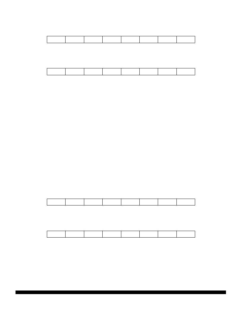
ATDSTAT —
ATD Status Register
$0066
Bit 7
6
5
4
3
2
1
Bit 0
SCF
0
0
0
0
CC2
CC1
CC0
RESET:
0
0
0
0
0
0
0
0
ATDSTAT
— ATD Status Register
$0067
Bit 7
6
5
4
3
2
1
Bit 0
CCF7
CCF6
CCF5
CCF4
CCF3
CCF2
CCF1
CCF0
RESET:
0
0
0
0
0
0
0
0
ATDTSTH
— ATD Test Register
$0068
Bit 7
6
5
4
3
2
1
Bit 0
SAR9
SAR8
SAR7
SAR6
SAR5
SAR4
SAR3
SAR2
RESET:
0
0
0
0
0
0
0
0
ATDTSTL
— ATD Test Register
$0069
Bit 7
6
5
4
3
2
1
Bit 0
SAR1
SAR0
RST
TSTOUT
TST3
TST2
TST1
TST0
RESET:
0
0
0
0
0
0
0
0
相關PDF資料 |
PDF描述 |
|---|---|
| MC68C912B32FU8 | 16-Bit Microcontroller |
| MC68B912B32FU8 | 16-Bit Microcontroller |
| MC68C912B32CFU8 | 16-Bit Microcontroller |
| MC68CK338 | Highly Integrated, Low-Power, 32-Bit Microcontroller |
| MC68EC060 | 32-Bit Microprocessors.(32位微處理器) |
相關代理商/技術參數 |
參數描述 |
|---|---|
| MC68B912B32FU8 | 制造商:MOTOROLA 制造商全稱:Motorola, Inc 功能描述:16-Bit Microcontroller |
| MC68BOOL | 制造商:MOTOROLA 制造商全稱:Motorola, Inc 功能描述:8-BIT MICROPROCESSING UNIT (MPU) |
| MC68BOOP | 制造商:MOTOROLA 制造商全稱:Motorola, Inc 功能描述:8-BIT MICROPROCESSING UNIT (MPU) |
| MC68BOOS | 制造商:MOTOROLA 制造商全稱:Motorola, Inc 功能描述:8-BIT MICROPROCESSING UNIT (MPU) |
| MC68C812A4 | 制造商:FREESCALE 制造商全稱:Freescale Semiconductor, Inc 功能描述:Technical Supplement MC68C812A4 3.3V Electrical Characteristics |
發布緊急采購,3分鐘左右您將得到回復。