- 您現在的位置:買賣IC網 > PDF目錄371046 > MC68B912B32 (Motorola, Inc.) 2.5V 100ppm/Degrees C, 50uA in SOT23-3 Series (Bandgap) Voltage Reference 3-SOT-23 -40 to 125 PDF資料下載
參數資料
| 型號: | MC68B912B32 |
| 廠商: | Motorola, Inc. |
| 英文描述: | 2.5V 100ppm/Degrees C, 50uA in SOT23-3 Series (Bandgap) Voltage Reference 3-SOT-23 -40 to 125 |
| 中文描述: | 16位微控制器 |
| 文件頁數: | 93/128頁 |
| 文件大小: | 748K |
| 代理商: | MC68B912B32 |
第1頁第2頁第3頁第4頁第5頁第6頁第7頁第8頁第9頁第10頁第11頁第12頁第13頁第14頁第15頁第16頁第17頁第18頁第19頁第20頁第21頁第22頁第23頁第24頁第25頁第26頁第27頁第28頁第29頁第30頁第31頁第32頁第33頁第34頁第35頁第36頁第37頁第38頁第39頁第40頁第41頁第42頁第43頁第44頁第45頁第46頁第47頁第48頁第49頁第50頁第51頁第52頁第53頁第54頁第55頁第56頁第57頁第58頁第59頁第60頁第61頁第62頁第63頁第64頁第65頁第66頁第67頁第68頁第69頁第70頁第71頁第72頁第73頁第74頁第75頁第76頁第77頁第78頁第79頁第80頁第81頁第82頁第83頁第84頁第85頁第86頁第87頁第88頁第89頁第90頁第91頁第92頁當前第93頁第94頁第95頁第96頁第97頁第98頁第99頁第100頁第101頁第102頁第103頁第104頁第105頁第106頁第107頁第108頁第109頁第110頁第111頁第112頁第113頁第114頁第115頁第116頁第117頁第118頁第119頁第120頁第121頁第122頁第123頁第124頁第125頁第126頁第127頁第128頁
MC68HC912B32
MC68HC912B32TS/D
MOTOROLA
93
13.3.3 SS Output
Available in master mode only, SS output is enabled with the SSOE bit in the SP0CR1 register if the
corresponding DDRS bit is set. The SS output pin will be connected to the SS input pin of the external
slave device. The SS output automatically goes low for each transmission to select the external device
and it goes high during each idling state to deselect external devices.
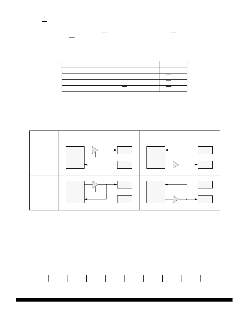
13.3.4 Bidirectional Mode (MOMI or SISO)
In bidirectional mode, the SPI uses only one serial data pin for external device interface. The MSTR bit
decides which pin to be used. The MOSI pin becomes serial data I/O (MOMI) pin for the master mode,
and the MISO pin becomes serial data I/O (SISO) pin for the slave mode. The direction of each serial
I/O pin depends on the corresponding DDRS bit.
Figure 24 Normal Mode and Bidirectional Mode
13.3.5 Register Descriptions
Control and data registers for the SPI subsystem are described below. The memory address indicated
for each register is the default address that is in use after reset. The entire 512-byte register block can
be mapped to any 2-Kbyte boundary within the standard 64-Kbyte address space. For more information
refer to
5 Operating Modes and Resource Mapping
.
Table 30 SS Output Selection
DDS7
0
0
1
1
SSOE
0
1
0
1
Master Mode
Slave Mode
SS Input
SS Input
SS Input
SS Input
SS Input with MODF Feature
Reserved
General-Purpose Output
SS Output
When SPE=1
Master Mode
MSTR=1
Slave Mode
MSTR=0
Normal
Mode
SPC0=0
SWOM enables open drain output.
SWOM enables open drain output.
Bidirectional
Mode
SPC0=1
SWOM enables open drain output. PS4 becomes GPIO.
SWOM enables open drain output. PS5 becomes GPIO.
SP0CR1
— SPI Control Register 1
$00D0
Bit 7
6
5
4
3
2
1
Bit 0
SPIE
SPE
SWOM
MSTR
CPOL
CPHA
SSOE
LSBF
RESET:
0
0
0
0
0
1
0
0
SPI
MO
MI
DDS5
Serial Out
Serial In
SPI
SI
SO
Serial In
Serial Out
DDS4
SPI
MOMI
PS4
DDS5
Serial Out
Serial In
SPI
PS5
SISO
DDS4
Serial In
Serial Out
相關PDF資料 |
PDF描述 |
|---|---|
| MC68C912B32FU8 | 16-Bit Microcontroller |
| MC68B912B32FU8 | 16-Bit Microcontroller |
| MC68C912B32CFU8 | 16-Bit Microcontroller |
| MC68CK338 | Highly Integrated, Low-Power, 32-Bit Microcontroller |
| MC68EC060 | 32-Bit Microprocessors.(32位微處理器) |
相關代理商/技術參數 |
參數描述 |
|---|---|
| MC68B912B32FU8 | 制造商:MOTOROLA 制造商全稱:Motorola, Inc 功能描述:16-Bit Microcontroller |
| MC68BOOL | 制造商:MOTOROLA 制造商全稱:Motorola, Inc 功能描述:8-BIT MICROPROCESSING UNIT (MPU) |
| MC68BOOP | 制造商:MOTOROLA 制造商全稱:Motorola, Inc 功能描述:8-BIT MICROPROCESSING UNIT (MPU) |
| MC68BOOS | 制造商:MOTOROLA 制造商全稱:Motorola, Inc 功能描述:8-BIT MICROPROCESSING UNIT (MPU) |
| MC68C812A4 | 制造商:FREESCALE 制造商全稱:Freescale Semiconductor, Inc 功能描述:Technical Supplement MC68C812A4 3.3V Electrical Characteristics |
發布緊急采購,3分鐘左右您將得到回復。