- 您現在的位置:買賣IC網 > PDF目錄371046 > MC68CK338 (Motorola, Inc.) Highly Integrated, Low-Power, 32-Bit Microcontroller PDF資料下載
參數資料
| 型號: | MC68CK338 |
| 廠商: | Motorola, Inc. |
| 元件分類: | 32位微控制器 |
| 英文描述: | Highly Integrated, Low-Power, 32-Bit Microcontroller |
| 中文描述: | 高度集成,低功耗,32位微控制器 |
| 文件頁數: | 41/133頁 |
| 文件大小: | 798K |
| 代理商: | MC68CK338 |
第1頁第2頁第3頁第4頁第5頁第6頁第7頁第8頁第9頁第10頁第11頁第12頁第13頁第14頁第15頁第16頁第17頁第18頁第19頁第20頁第21頁第22頁第23頁第24頁第25頁第26頁第27頁第28頁第29頁第30頁第31頁第32頁第33頁第34頁第35頁第36頁第37頁第38頁第39頁第40頁當前第41頁第42頁第43頁第44頁第45頁第46頁第47頁第48頁第49頁第50頁第51頁第52頁第53頁第54頁第55頁第56頁第57頁第58頁第59頁第60頁第61頁第62頁第63頁第64頁第65頁第66頁第67頁第68頁第69頁第70頁第71頁第72頁第73頁第74頁第75頁第76頁第77頁第78頁第79頁第80頁第81頁第82頁第83頁第84頁第85頁第86頁第87頁第88頁第89頁第90頁第91頁第92頁第93頁第94頁第95頁第96頁第97頁第98頁第99頁第100頁第101頁第102頁第103頁第104頁第105頁第106頁第107頁第108頁第109頁第110頁第111頁第112頁第113頁第114頁第115頁第116頁第117頁第118頁第119頁第120頁第121頁第122頁第123頁第124頁第125頁第126頁第127頁第128頁第129頁第130頁第131頁第132頁第133頁
MC68CK338
MC68CK338TS/D
MOTOROLA
41
Data bus pin 9 controls the state of this register following reset. If DATA9 is set to one during reset, the
register is set to $FF, which defines all port F pins as interrupt request inputs. If DATA9 is cleared to
zero during reset, this register is set to $00, defining all port F pins as I/O pins.
3.8 Resets
Reset procedures handle system initialization and recovery from catastrophic failure. The MCU per-
forms resets with a combination of hardware and software. The SIML determines whether a reset is val-
id, asserts control signals, performs basic system configuration based on hardware mode-select inputs,
then passes control to the CPU.
Reset occurs when an active low logic level on the RESET pin is clocked into the SIML. Resets are gat-
ed by the CLKOUT signal. Asynchronous resets are assumed to be catastrophic. An asynchronous re-
set can occur on any clock edge. Synchronous resets are timed to occur at the end of bus cycles. If
there is no clock when RESET is asserted, reset does not occur until the clock starts. Resets are
clocked in order to allow completion of write cycles in progress at the time RESET is asserted.
Reset is the highest-priority CPU32L exception. Any processing in progress is aborted by the reset ex-
ception, and cannot be restarted. Only essential tasks are performed during reset exception processing.
Other initialization tasks must be accomplished by the exception handler routine.
3.8.1 SIML Reset Mode Selection
The logic states of certain data bus pins during reset determine SIML operating configuration. In addi-
tion, the state of the MODCLK pin determines system clock source and the state of the BKPT pin de-
termines what happens during subsequent breakpoint assertions.
Table 31
is a summary of reset mode
selection options.
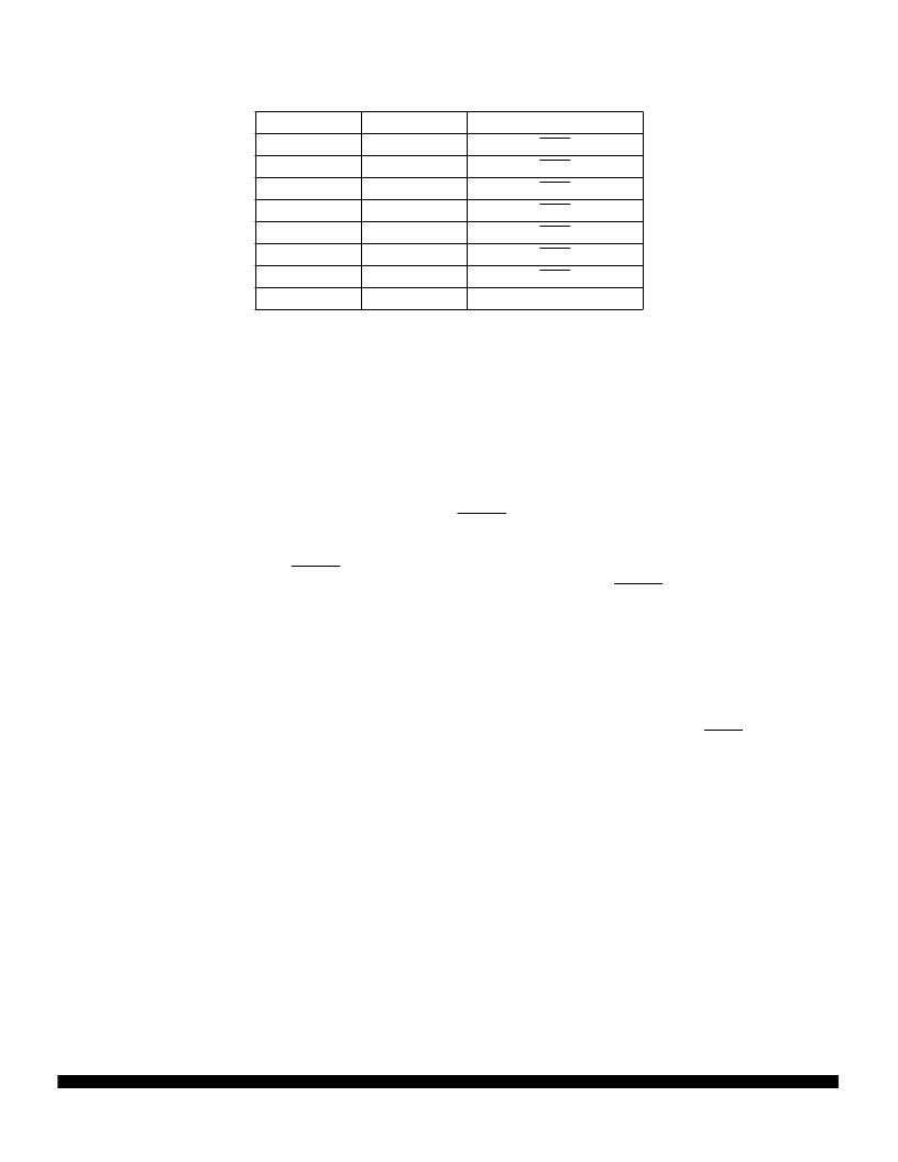
Table 30 Port F Pin Assignments
PFPAR Field
PFPA7
PFPA6
PFPA5
PFPA4
PFPA3
PFPA2
PFPA1
PFPA0
Port F Signal
PF7
PF6
PF5
PF4
PF3
PF2
PF1
PF0
Alternate Signal
IRQ7
IRQ6
IRQ5
IRQ4
IRQ3
IRQ2
IRQ1
MODCLK
相關PDF資料 |
PDF描述 |
|---|---|
| MC68EC060 | 32-Bit Microprocessors.(32位微處理器) |
| MC68EN360RC25V | QUad Integrated Communications Controller Users Manual |
| MC68EN360CFE25 | QUad Integrated Communications Controller Users Manual |
| MC68EN360FE25 | AC 4C 4#12 PIN PLUG 023 |
| MC68EN360FE25V | QUad Integrated Communications Controller Users Manual |
相關代理商/技術參數 |
參數描述 |
|---|---|
| MC68CK338CPV14 | 制造商:Rochester Electronics LLC 功能描述:- Bulk |
| MC68CK338CPV14B1 | 制造商:FREESCALE 制造商全稱:Freescale Semiconductor, Inc 功能描述:32-Bit Modular Microcontroller |
| MC68CM16Z1 | 制造商:FREESCALE 制造商全稱:Freescale Semiconductor, Inc 功能描述:M68HC16Z Series |
| MC68CM16Z1CFC16 | 制造商:FREESCALE 制造商全稱:Freescale Semiconductor, Inc 功能描述:M68HC16Z Series |
| MC68CM16Z1CPV16 | 制造商:FREESCALE 制造商全稱:Freescale Semiconductor, Inc 功能描述:M68HC16Z Series |
發布緊急采購,3分鐘左右您將得到回復。