- 您現在的位置:買賣IC網 > PDF目錄371046 > MC68CK338 (Motorola, Inc.) Highly Integrated, Low-Power, 32-Bit Microcontroller PDF資料下載
參數資料
| 型號: | MC68CK338 |
| 廠商: | Motorola, Inc. |
| 元件分類: | 32位微控制器 |
| 英文描述: | Highly Integrated, Low-Power, 32-Bit Microcontroller |
| 中文描述: | 高度集成,低功耗,32位微控制器 |
| 文件頁數: | 85/133頁 |
| 文件大小: | 798K |
| 代理商: | MC68CK338 |
第1頁第2頁第3頁第4頁第5頁第6頁第7頁第8頁第9頁第10頁第11頁第12頁第13頁第14頁第15頁第16頁第17頁第18頁第19頁第20頁第21頁第22頁第23頁第24頁第25頁第26頁第27頁第28頁第29頁第30頁第31頁第32頁第33頁第34頁第35頁第36頁第37頁第38頁第39頁第40頁第41頁第42頁第43頁第44頁第45頁第46頁第47頁第48頁第49頁第50頁第51頁第52頁第53頁第54頁第55頁第56頁第57頁第58頁第59頁第60頁第61頁第62頁第63頁第64頁第65頁第66頁第67頁第68頁第69頁第70頁第71頁第72頁第73頁第74頁第75頁第76頁第77頁第78頁第79頁第80頁第81頁第82頁第83頁第84頁當前第85頁第86頁第87頁第88頁第89頁第90頁第91頁第92頁第93頁第94頁第95頁第96頁第97頁第98頁第99頁第100頁第101頁第102頁第103頁第104頁第105頁第106頁第107頁第108頁第109頁第110頁第111頁第112頁第113頁第114頁第115頁第116頁第117頁第118頁第119頁第120頁第121頁第122頁第123頁第124頁第125頁第126頁第127頁第128頁第129頁第130頁第131頁第132頁第133頁
MC68CK338
MC68CK338TS/D
MOTOROLA
85
IARB[2:0] — Interrupt Arbitration Field
This bit field and the IARB3 bit within each submodule provide 15 different interrupt arbitration numbers
that can be used to arbitrate between interrupt requests occurring on the IMB with the same interrupt
priority level.
The IARB field defaults to zero on reset, preventing the module from arbitrating during an IACK cycle.
If no arbitration takes place during the IACK cycle, the SIML generates a spurious interrupt, indicating
to the system that the interrupt arbitration number has not been initialized.
The CTM6 allows two different arbitration numbers to be used by providing each submodule with its own
IARB3 bit (which can be set or cleared in software). Once IARB[2:0] are assigned in the BIUSM, they
apply to all CTM6 interrupt requests. Therefore, CTM6 submodule interrupts can be prioritized with re-
quests from other modules at the same interrupt level. IARB[2:0] are cleared by reset.
Bits[7:6], [4:1] — Not Implemented
TBRS1, TBRS0 — Time Base Register Bus Select Bits
These bits specify which time base bus is accessed when the time base register (BIUTBR) is read. Re-
fer to
Table 48
.
BIUTEST —
BIUSM Test Register
BIUTEST is used during factory testing of the CTM6. Accesses to BIUTEST must be made while the
MCU is in test mode.
$YFF402
BIUTBR is a read-only register used to read the value present on one of the time base buses. The time
base bus being accessed is determined by TBRS1 and TBRS0 in BIUMCR. Writing to BIUTBR has no
effect during normal operation.
6.5 Counter Prescaler Submodule (CPSM)
The counter prescaler submodule (CPSM) is a programmable divider system that provides the CTM6
counters with a choice of six clock signals (PCLKx) derived from the sixth frequency MCU system clock
(f
sys
). Five of these frequencies are derived from a fixed divider chain. The divide ratio is software se-
lectable from a choice of four divide ratios.
The CPSM is contained within the BIUSM.
Figure 19
shows a block diagram of the CPSM.
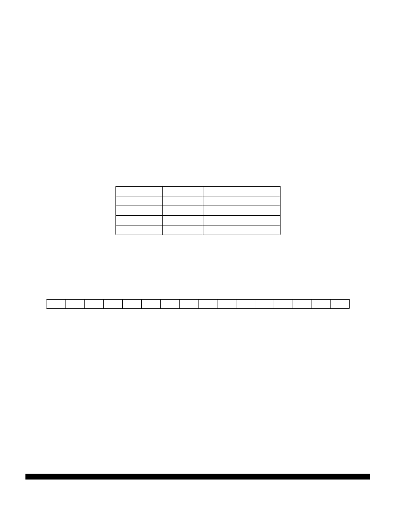
Table 48 Time Base Register Bus Select Bits
TBRS1
0
0
1
1
TBRS0
0
1
0
1
Time Base Bus
TBB1
TBB2
TBB3
TBB4
BIUTBR —
BIUSM Time Base Register
$YFF404
15
14
13
12
11
10
9
8
7
6
5
4
3
2
1
0
RESET:
0
0
0
0
0
0
0
0
0
0
0
0
0
0
0
0
相關PDF資料 |
PDF描述 |
|---|---|
| MC68EC060 | 32-Bit Microprocessors.(32位微處理器) |
| MC68EN360RC25V | QUad Integrated Communications Controller Users Manual |
| MC68EN360CFE25 | QUad Integrated Communications Controller Users Manual |
| MC68EN360FE25 | AC 4C 4#12 PIN PLUG 023 |
| MC68EN360FE25V | QUad Integrated Communications Controller Users Manual |
相關代理商/技術參數 |
參數描述 |
|---|---|
| MC68CK338CPV14 | 制造商:Rochester Electronics LLC 功能描述:- Bulk |
| MC68CK338CPV14B1 | 制造商:FREESCALE 制造商全稱:Freescale Semiconductor, Inc 功能描述:32-Bit Modular Microcontroller |
| MC68CM16Z1 | 制造商:FREESCALE 制造商全稱:Freescale Semiconductor, Inc 功能描述:M68HC16Z Series |
| MC68CM16Z1CFC16 | 制造商:FREESCALE 制造商全稱:Freescale Semiconductor, Inc 功能描述:M68HC16Z Series |
| MC68CM16Z1CPV16 | 制造商:FREESCALE 制造商全稱:Freescale Semiconductor, Inc 功能描述:M68HC16Z Series |
發布緊急采購,3分鐘左右您將得到回復。