- 您現在的位置:買賣IC網 > PDF目錄382347 > MR82510 (Intel Corp.) ASYNCHRONOUS SERIAL CONTROLLER PDF資料下載
參數資料
| 型號: | MR82510 |
| 廠商: | Intel Corp. |
| 英文描述: | ASYNCHRONOUS SERIAL CONTROLLER |
| 中文描述: | 異步串行控制器 |
| 文件頁數: | 2/40頁 |
| 文件大小: | 463K |
| 代理商: | MR82510 |
第1頁當前第2頁第3頁第4頁第5頁第6頁第7頁第8頁第9頁第10頁第11頁第12頁第13頁第14頁第15頁第16頁第17頁第18頁第19頁第20頁第21頁第22頁第23頁第24頁第25頁第26頁第27頁第28頁第29頁第30頁第31頁第32頁第33頁第34頁第35頁第36頁第37頁第38頁第39頁第40頁
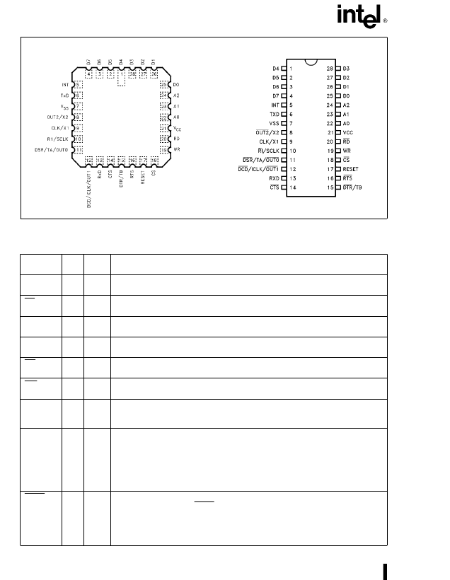
M82510
28-Pad LCC
271072–55
28-Pin Cerdip
271072–2
Figure 2. Package Pinouts
M82510 PINOUT DEFINITION
Symbol
Pin
No.
Type
Name and Description
RESET
17
I
RESET:
A high on this input pin resets the M82510 to the Default Wake-up
mode.
CS
18
I
CHIP SELECT:
A low on this input pin enables the M82510 and allows read or
write operations.
A2–A0
24-
22
4
*
25
I
ADDRESS PINS:
These inputs interface with three bits of the System Address
Bus to select one of the internal registers for read or write.
D7–D0
I/O
DATA BUS:
Bidirectional, three state, eight-bit Data Bus. These pins allow
transfer of bytes between the CPU and the M82510.
RD
20
I
READ:
A low on this input pin allows the CPU to read Data or Status bytes from
the M82510.
WR
19
I
WRITE:
A low on this input allows the CPU to write Data or Control bytes to the
M82510.
INT
5
O
INTERRUPT:
A high on this output pin signals an interrupt request to the CPU.
The CPU may determine the particular source and cause of the interrupt by
reading the M82510 Status registers.
CLK/X1
9
I
MULTIFUNCTION:
This input pin serves as a source for the internal system
clock. The clock may be asynchronous to the serial clocks and to the processor
clock. This pin may be used in one of two modes: CLK D in this mode an
externally generated TTL compatible clock should be used to drive this input pin;
X1 D in this mode the clock is internally generated by an on-chip crystal
oscillator. This mode requires a crystal to be connected between this pin (X1)
and the X2 pin. (See System Clock Generation.)
OUT2/X2
8
O
MULTIFUNCTION:
This is a dual function pin which may be configured to one of
the following functions: OUT2 D a general purpose output pin controlled by the
CPU, only available when CLK/X1 pin is driven by an externally generated clock;
X2 - this pin serves as an output pin for the crystal oscillator.Note: The
configuration of the pin is done only during hardware reset. For more details
refer to the System Clock Generation.
*
Pins 28–25 and Pins 4–1.
2
相關PDF資料 |
PDF描述 |
|---|---|
| MR8251A | PROGRAMMABLE COMMUNICATION INTERFACE |
| MR851G | Axial Lead Fast Recovery Rectifiers |
| MR851RL | Axial Lead Fast Recovery Rectifiers |
| MR851RLG | Axial Lead Fast Recovery Rectifiers |
| MR852G | Axial Lead Fast Recovery Rectifiers |
相關代理商/技術參數 |
參數描述 |
|---|---|
| MR82510/B | 制造商:Rochester Electronics LLC 功能描述: |
| MR8251A | 制造商:Intel 功能描述: |
| MR8251A/B | 制造商:Rochester Electronics LLC 功能描述: |
| MR8254/B | 制造商:Rochester Electronics LLC 功能描述: |
| MR8254/R | 制造商:Rochester Electronics LLC 功能描述:- Bulk |
發布緊急采購,3分鐘左右您將得到回復。