- 您現在的位置:買賣IC網 > PDF目錄382347 > MR82510 (Intel Corp.) ASYNCHRONOUS SERIAL CONTROLLER PDF資料下載
參數資料
| 型號: | MR82510 |
| 廠商: | Intel Corp. |
| 英文描述: | ASYNCHRONOUS SERIAL CONTROLLER |
| 中文描述: | 異步串行控制器 |
| 文件頁數: | 37/40頁 |
| 文件大小: | 463K |
| 代理商: | MR82510 |
第1頁第2頁第3頁第4頁第5頁第6頁第7頁第8頁第9頁第10頁第11頁第12頁第13頁第14頁第15頁第16頁第17頁第18頁第19頁第20頁第21頁第22頁第23頁第24頁第25頁第26頁第27頁第28頁第29頁第30頁第31頁第32頁第33頁第34頁第35頁第36頁當前第37頁第38頁第39頁第40頁
M82510
AC SPECIFICATIONS
(Over Specified Operating Conditions)
Testing Conditions:
#
All AC output parameters are under output load
of 20 to 100 pF, unless otherwise specified.
#
AC testing inputs are driven at 2.4V for logic ‘1’
on CERDIP, 2.7V on LCC, and 0.45V for logic
‘0’. Output timing measurements are made at
1.5V for both a logical ‘0’ and ‘1’.
#
In the following tables, the units are ns, unless
otherwise specified.
System Interface SpecificationDSystem Clock
Specification:
The M82510 system clock is supplied via the CLK
pin or generated by an on-chip crystal oscillator. The
clock is optionally divided by two. The CLK parame-
ters are given separately for internal divide-by-two
option ACTIVE and INACTIVE.
The system clock (after division by two, if active)
must be at least 16X the Tx or Rx baud rate (the
faster of the two).
SYSTEM CLOCK SPECIFICATIONS
Symbol
Parameter
Min
Max
Notes
DIVIDE BY TWO OPTIONDACTIVE
T
CY
/2
CLK Period
54
250
(2)
TCLCH
CLK Low Time
25
TCHCL
CLK High Time
25
TCH1CH2
CLK Rise Time
10
(1)
TCL2CL1
CLK Fall Time
10
(1)
FXTAL
External Crystal
Frequency Rating
4.0
18.432
MHz
DIVIDE BY TWO OPTIONDINACTIVE
T
CY
CLK Period
108
TCLCH
CLK Low Tme
54
TCHCL
CLK High Time
44
250
TCH1CH2
CLK Rise Time
15
(1)
TCL2CL1
CLK Fall Time
15
(1)
NOTES:
1. Rise/fall times are measured between 0.8 and 2.0V.
2. Tcy in ACTIVE divide by two option is TWICE the input
clock period.
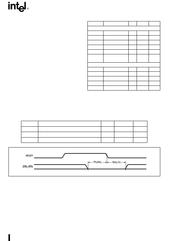
RESET SPECIFICATION
Symbol
Parameter
Min
Max
Notes
TRSHL
Reset WidthDCLK/X1 Configured to CLK
8 T
CY
(1)
TTLRSL
RTS/DTR LOW Setup to Reset Inactive
6 T
CY
(2)
TRSLTX
RTS/DTR Low Hold after Reset Inactive
0
T
CY
b
20
(2)
271072–49
NOTES:
1. In case of CLK/X1 configured as X1, 1 Ms is required to guarantee crystal oscillator wake-up.
2. RTS/DTR are internally driven HIGH during RESET active time. The pin should be either left OPEN or externally driven
LOW during RESET according to the required configuration of the system clock. These parameters specify the timing re-
quirements on these pins, in case they are externally driven LOW during RESET.
The maximum spec on TRSLTX requires that the RTS/DTR pins not be forced later than TRSLTX maximum.
37
相關PDF資料 |
PDF描述 |
|---|---|
| MR8251A | PROGRAMMABLE COMMUNICATION INTERFACE |
| MR851G | Axial Lead Fast Recovery Rectifiers |
| MR851RL | Axial Lead Fast Recovery Rectifiers |
| MR851RLG | Axial Lead Fast Recovery Rectifiers |
| MR852G | Axial Lead Fast Recovery Rectifiers |
相關代理商/技術參數 |
參數描述 |
|---|---|
| MR82510/B | 制造商:Rochester Electronics LLC 功能描述: |
| MR8251A | 制造商:Intel 功能描述: |
| MR8251A/B | 制造商:Rochester Electronics LLC 功能描述: |
| MR8254/B | 制造商:Rochester Electronics LLC 功能描述: |
| MR8254/R | 制造商:Rochester Electronics LLC 功能描述:- Bulk |
發布緊急采購,3分鐘左右您將得到回復。