- 您現在的位置:買賣IC網 > PDF目錄382369 > P90CL301BFH (NXP SEMICONDUCTORS) Low voltage 16-bit microcontroller PDF資料下載
參數資料
| 型號: | P90CL301BFH |
| 廠商: | NXP SEMICONDUCTORS |
| 元件分類: | 微控制器/微處理器 |
| 英文描述: | Low voltage 16-bit microcontroller |
| 中文描述: | 16-BIT, 27.02 MHz, MICROCONTROLLER, PQFP80 |
| 文件頁數: | 12/92頁 |
| 文件大小: | 526K |
| 代理商: | P90CL301BFH |
第1頁第2頁第3頁第4頁第5頁第6頁第7頁第8頁第9頁第10頁第11頁當前第12頁第13頁第14頁第15頁第16頁第17頁第18頁第19頁第20頁第21頁第22頁第23頁第24頁第25頁第26頁第27頁第28頁第29頁第30頁第31頁第32頁第33頁第34頁第35頁第36頁第37頁第38頁第39頁第40頁第41頁第42頁第43頁第44頁第45頁第46頁第47頁第48頁第49頁第50頁第51頁第52頁第53頁第54頁第55頁第56頁第57頁第58頁第59頁第60頁第61頁第62頁第63頁第64頁第65頁第66頁第67頁第68頁第69頁第70頁第71頁第72頁第73頁第74頁第75頁第76頁第77頁第78頁第79頁第80頁第81頁第82頁第83頁第84頁第85頁第86頁第87頁第88頁第89頁第90頁第91頁第92頁
1996 Dec 11
12
Philips Semiconductors
Preliminary specification
Low voltage 16-bit microcontroller
P90CL301BFH (C100)
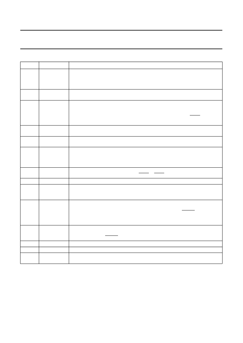
Table 14
Description of SYSCON bits
BIT
SYMBOL
DESCRIPTION
15
WDSC
Bus error Watchdog short cycle
. WDSC = 0 for normal mode; the bus error Watchdog
counts 2048 periods before activating the bus error sequence. WDSC = 1 for Bus error
Watchdog short cycle; the Watchdog counts 16 periods before activating the bus error
sequence.
Bus pull-up enable
. If BPE = 0, the Address and Data bus internal pull-ups are switched
off. If BPE = 1, the Address and Data bus internal pull-ups are switched on.
Invert bus size for chip select boot and mode of port P0 to P7
. CSBTX = 0 for normal
mode; bus size is defined by the pin BSIZE. If CSBTX = 1, the chip select boot is defined
by the inverted value of the pin BSIZE. The mode change should be executed from the
internal RAM or from a memory activated by any other chip select than CSBT. For further
details see also Section 6.3.
CPU Standby mode
. STBY = 0, for normal mode. STBY = 1, for Standby mode; only the
CPU clock is switched off, the peripheral clocks are still running (see Fig.4).
Prescaler for primary peripheral clock (FCLK) and the UART clock in mode 0
.
The CPU clock = CLK; FCLK =
1
divisor
×
CLK. See Table 15 for the divisor values.
Prescaler for secondary peripheral clock FCLK2
(derived from the primary peripheral
clock FCLK), used for the ADC; the maximum value of the FCLK2 clock is dependent on
the supply voltage V
DD
; see Section 19. If PCLK2 = 0, then FCLK is divided by 2;
if PCLK2 = 1, then FCLK is divided by 4.
If PDE = 0, then bits A22 to A19 are in normal operation; If PDE =1, then bits A22 to A19
are used as 8051 peripheral chip-select PCS3 to PCS0.
General purpose flag bit
; reset to a logic 0 after CPU reset.
For IM = 0, level 7 is loaded into the Status Register during interrupt processing to
prevent the CPU from being interrupted by another interrupt source. For IM = 1, the
current interrupt level is loaded into the Status Register allowing nested interrupts.
For WD = 0, the time-out for bus error detection is switched off. If the time-out is not
used, the Watchdog Timer can be used to stop a non-acknowledged bus transfer.
For WD = 1, the time-out for bus error detection is activated. If no DTACK has been sent
by the addressed device after 128
×
16 internal clock cycles the on-chip bus error signal
is activated.
FBC = 0, normal bus cycle; FBC = 1, fast bus cycle. An external read bus cycle can take
a minimum of 3 clock periods; the minimum write cycle is still 4 clock periods; in order to
get this access time DTACK should be asserted on time.
PD = 0, for normal mode; PD = 1, for Power-down mode (see Section 6.8).
IDL = 0, for normal mode; IDL = 1, for Idle mode (see Section 6.8).
DOFF = 0, for normal mode. DOFF = 1, for delay counter off; if set at wake-up from
Power-down the delay counter waiting period is skipped.
14
BPE
13
CSBTX
12
STBY
11, 7
and 6
10
PCLK3, PCLK1
and PCLK0
PCLK2
9
PDE
8
5
GF
IM
4
WD
3
FBC
2
1
0
PD
IDL
DOFF
相關PDF資料 |
PDF描述 |
|---|---|
| P93U422-35DC | x4 SRAM |
| P93U422-35DM | x4 SRAM |
| P93U422-35DMB | x4 SRAM |
| P93U422-35LC | x4 SRAM |
| P93U422-35LM | x4 SRAM |
相關代理商/技術參數 |
參數描述 |
|---|---|
| P-90-F | 制造商:Hozan Tool Industrial Co Ltd 功能描述: |
| P90PCT101PC | 制造商:PERFORMANCE/ 功能描述:90PCT101PC |
| P-910 | 制造商:Hozan Tool Industrial Co Ltd 功能描述: |
| P9-100001 | 制造商:OTTO Engineering Inc 功能描述:P9-111122 EX H20 |
| P9-100002 | 制造商:OTTO Engineering Inc 功能描述:P9-111129 EX. |
發布緊急采購,3分鐘左右您將得到回復。